Portable electronic device and circuit transferring method

An electronic device, portable technology, applied in the direction of conductive pattern formation, containing printed electrical components, etc., can solve the problems of product cost reduction, product elasticity reduction, volume reduction, etc., to save inventory management man-hours and costs, Improves flexibility and saves assembly steps

Inactive Publication Date: 2009-06-10
ASUSTEK COMPUTER INC
View PDF0 Cites 0 Cited by
  • Summary
  • Abstract
  • Description
  • Claims
  • Application Information

AI Technical Summary

Problems solved by technology

[0004] 1. It takes a lot of components to complete the circuit components, and the resulting labor and material costs and inventory management costs make it impossible to reduce product costs
[0005] 2. Multiple assembly processes are required to assemble circuit components to electronic devices, and the resulting assembly man-hours make it impossible to reduce product costs
[0006] 3. A large number of assembly parts makes the volume of the product unable to be reduced and reduces the flexibility of product design. For example, if the design of circuit components is changed, the spatial distribution and connection relationship of the surrounding assembly parts must also be considered, which reduces the design flexibility. Elasticity on

Method used


Image

  • Portable electronic device and circuit transferring method
  • Portable electronic device and circuit transferring method
  • Portable electronic device and circuit transferring method

Examples


no. 1 example

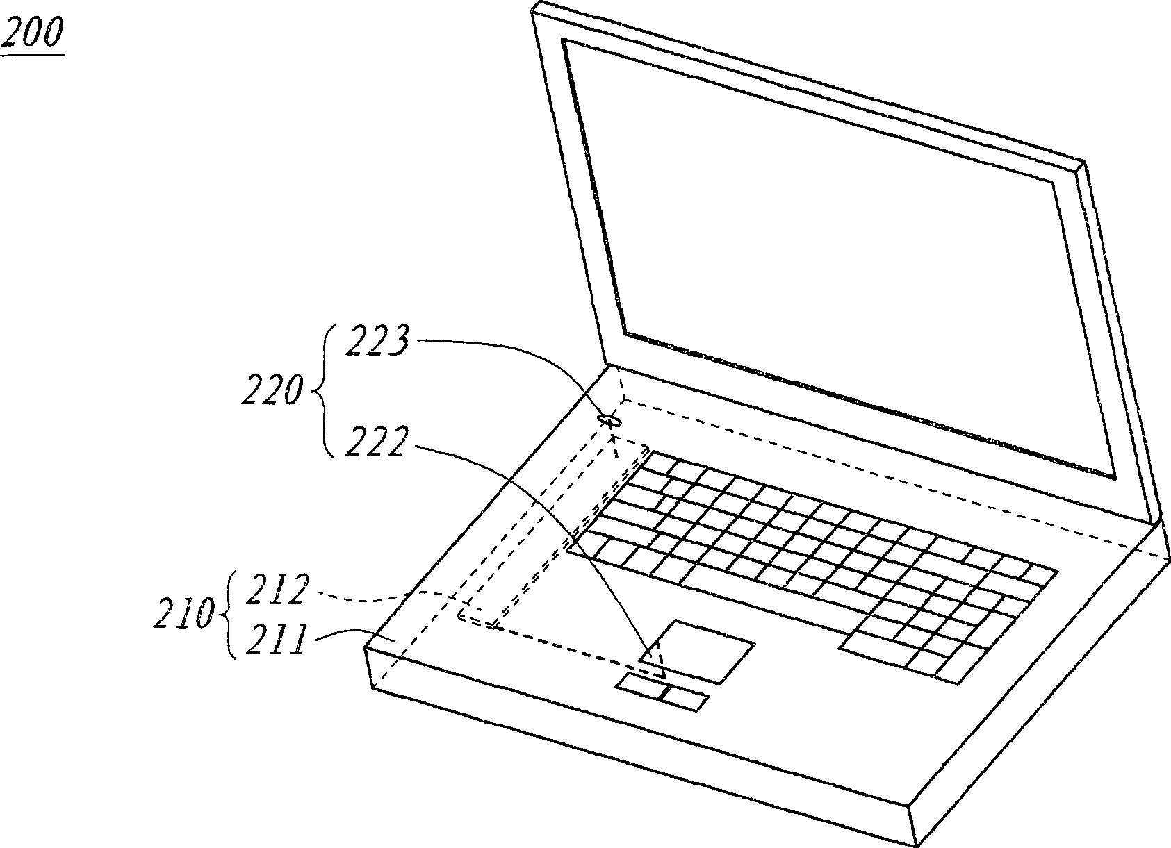
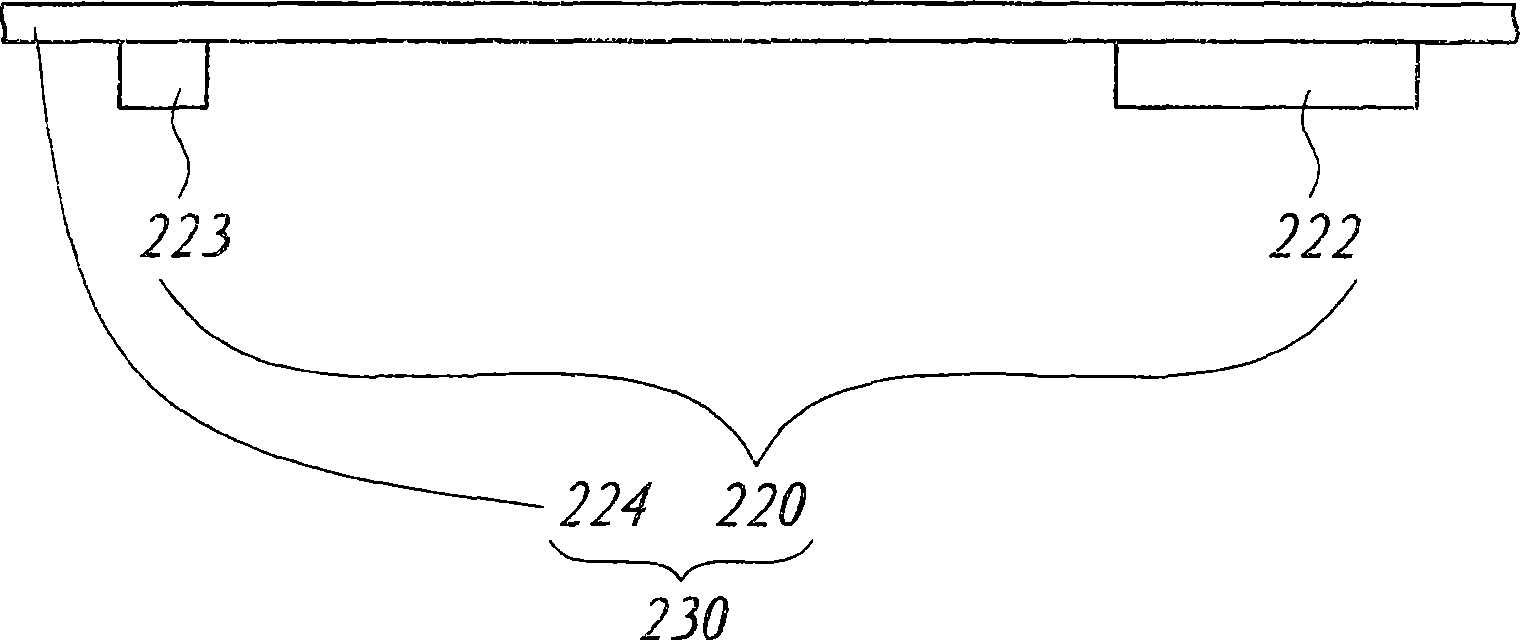
[0030] Please refer to figure 1 , which is a schematic perspective view of the portable electronic device 200 according to the first embodiment of the present invention. The portable electronic device 200 includes a body 210 and a circuit element 220 . The body 210 has a shell wall 211 and a control element 212 . The circuit element 220 is electrically connected to the control element 212 . The circuit element 220 and the casing wall 211 are integrally formed by pad printing. The circuit element 220 of this embodiment includes a sensing element 222 and a light emitting element 223 . The sensing element 222 is a touch pad, and the light emitting element 223 is an indicator light.

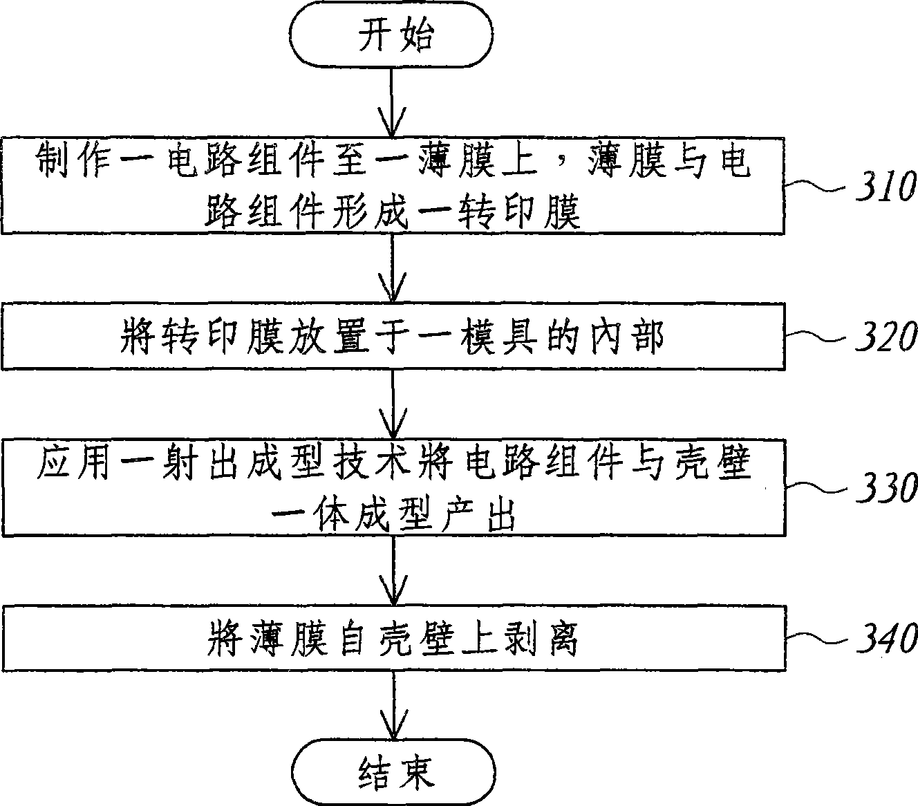
[0031] Please refer to figure 2 . figure 2 Shown is a schematic flow chart of a circuit element pad printing method. In step 310 , fabricating circuit elements on a thin film, so that the thin film and the circuit elements form a transfer film. Step 320 places the transfer film inside a mold....

no. 2 example

[0046] Please refer to Figure 9 , which is a schematic flow chart of a pad printing method for circuit components. The difference between this embodiment and the first embodiment lies in that the integral molding is completed by using a thermal transfer printing technology. Such as Figure 9 As shown, in step 910, fabricate circuit elements on a thin film, so that the thin film and the circuit elements form a transfer film. In step 920, thermal transfer technology is used to pad print the circuit element on the casing wall, so that the circuit element and the casing wall are integrally formed and produced. Step 930 peels the film from the shell wall.

[0047] Please refer to Figure 10 , which is shown as Figure 9 A schematic diagram of pad-printing the circuit element 821 onto the shell wall 811 by applying thermal transfer technology in step 920 of FIG. In step 920 , thermal transfer technology is applied, that is, a heat energy and a pressure are applied to the tran...


PUM


Abstract

The present invention relates to a portable type electronic device and a circuit component bat printing method thereof. The portable type electronic device comprises a body and a circuit component, wherein the body is provided with a shell wall and a control component. The circuit component and the shell wall are integrated by a bat printing mode and the circuit component is electrically connected with the control component.

Description

technical field [0001] The present invention relates to a portable electronic device and its circuit component pad printing method, and in particular to a portable electronic device with the circuit component integrated on the shell wall and its circuit component pad printing method. Background technique [0002] In the era of rapid technological development, portable electronic devices, such as a notebook computer, a communication mobile phone, a personal digital assistant (PDA), a PDA mobile phone or a global positioning system (global positioning system), etc. Devices have become an integral part of modern life. Its easy-to-carry feature allows users to communicate with other people by voice or data processing anytime, anywhere. [0003] However, in order to operate various functions of the portable electronic device, such as signal transmission and reception, data access or display light emission, etc., a certain number of circuit elements must be installed in the porta...

Claims


Application Information

Patent Timeline
IPC IPC(8): H05K1/16H05K3/10
Inventor 陈泓翔邱杨博
Owner ASUSTEK COMPUTER INC
Why Eureka
Try Eureka