Anode construction for top light emitting organic display and manufacturing process thereof

A technology of anode structure and manufacturing process, applied in the field of anode structure and manufacturing process of top-emitting organic display, can solve the problems of high resistance, low luminous efficiency, increased heat generation and power consumption, etc.

Active Publication Date: 2009-06-17
YUNNAN NORTH OLIGHTEK OPTO ELECTRONICS TECH
View PDF0 Cites 14 Cited by
  • Summary
  • Abstract
  • Description
  • Claims
  • Application Information

AI Technical Summary

Problems solved by technology

[0004] What the present invention is to solve is that indium oxide-tin (ITO) is used as a raw material, and the surface of the anode electrode formed by radio frequency sputtering method is not smooth, the luminous efficiency is low, the resistance is large, and the problems of increasing heat production and power consumption

Method used


Image

  • Anode construction for top light emitting organic display and manufacturing process thereof

Examples


Embodiment 1

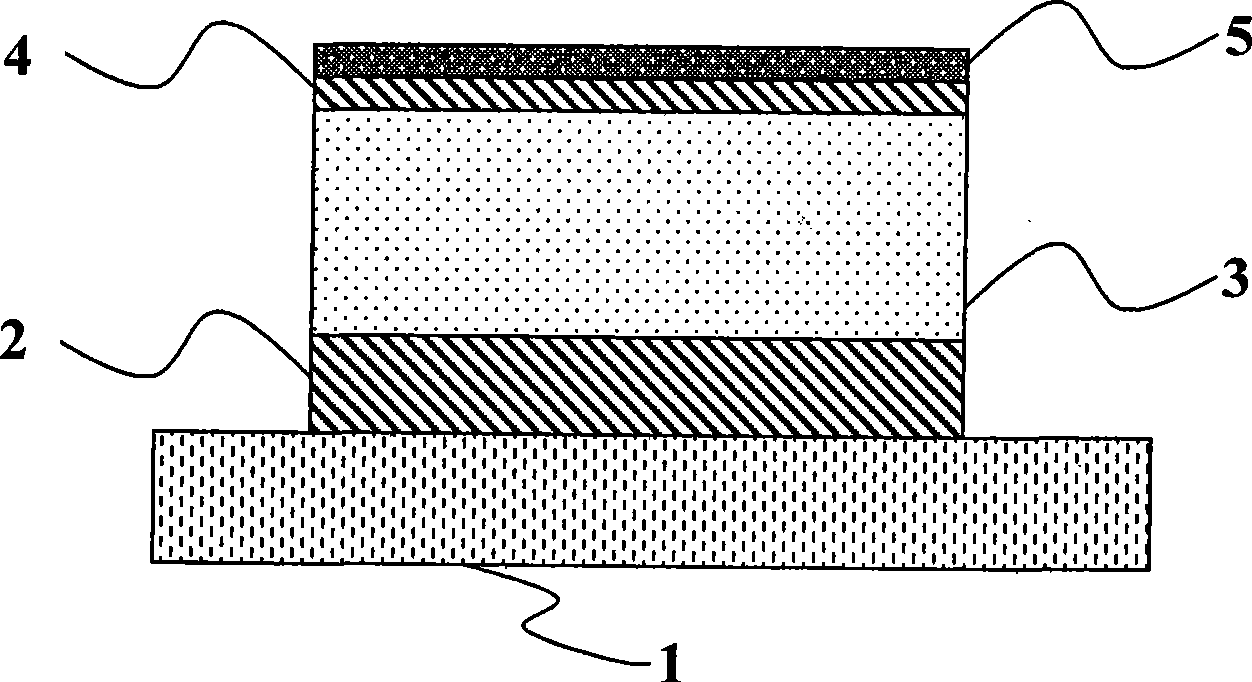
[0020] Example 1: An anode structure of a top-emission organic display uses silicon as a substrate to form a silicon substrate layer 1, uses chromium, aluminum and molybdenum materials to form a film-coated electrode body, and forms a high-purity chromium film layer 2 on the silicon substrate layer 1 A four-layer film anode structure of a high-purity aluminum film layer 3 , a high-purity chromium film layer 4 and a high-purity molybdenum film layer 5 .

[0021] If implemented by electron beam evaporation, it will include the following processes:

[0022] 1. Before coating, preheat the silicon substrate layer 1, the preheating temperature is 85°C, and the vacuum degree of the evaporation chamber is 10 -5 Pa;

[0023] 2. For metal coating, the order of evaporation is high-purity chromium, high-purity aluminum, high-purity chromium, and high-purity molybdenum. The steps of evaporation are as follows:

[0024] A, silicon substrate layer 1 is preheated;

[0025] B, vapor-deposit...


PUM


Abstract

Disclosed are an anode structure of a top-emitting organic display and a manufacturing process thereof, and relates to a top-emitting organic light-emitting device, in particular to a low resistivity anode structure applied to a top-emitting organic display and a manufacturing process thereof. The anode structure of the top-emitting organic display includes forming an electrode via coating films on a silicon substrate, which is characterized in that four layers of films are coated on the silicon substrate, namely a high purity chromium film layer, a high purity aluminum film layer, a high purity chromium film layer and a high purity aluminum film layer from the silicon substrate layer to the top, besides radio-frequency sputtering process, PVD process is utilized, and pre-heating treatment and metal coating process are performed on the silicon substrate. The novel anode structure has high conductivity and economical property and is easy to be coated, the OLED light emitting efficiency of the novel anode structure is increased to 30% due to the relatively low absorption coefficient of light and higher reflection coefficient of light, and thereby the performance of the novel anode structure is superior to the existing anode structure.

Description

technical field [0001] An organic electroluminescent device, especially a low-resistivity anode structure and its manufacturing process used in top-emission organic displays. Background technique [0002] Top-emitting organic display (OLED) has many advantages such as full solid state, active light emission, high contrast ratio, ultra-thin, low power consumption, no viewing angle limitation, fast response, shock resistance, wide working range, and easy realization of flexible display and 3D display. , Gradually become the fastest growing new display technology in the next 20 years. [0003] A conventional top-emitting OLED structure, like other OLED structures, consists of an anode (first electrode), a cathode (second electrode), and an organic light-emitting layer between the anode and cathode. The light-emitting mechanism and process of OLED is to inject electrons and holes from the cathode and anode respectively. The injected electrons and holes are transported in the or...

Claims


Application Information

Patent Timeline
Patent Type & Authority Applications(China)
IPC IPC(8): H01L51/52H01L51/54H01L51/56
CPCH01L51/5218H10K50/818
Inventor 邓荣斌季华夏
Owner YUNNAN NORTH OLIGHTEK OPTO ELECTRONICS TECH
Why Eureka
Try Eureka