Method and apparatus for diagnosing and correcting basal lamina offset

A correction method and technology of a correction device, applied in the field of microelectronics, can solve the problems of high implementation cost, microprocessing chips and electronic components are not suitable for high temperature and vacuum environment, a large number of complex image processing algorithms, etc. Sheet damage and production loss, the effect of improving accuracy

Active Publication Date: 2009-06-24
安徽尚特杰企业管理有限公司
View PDF1 Cites 17 Cited by
  • Summary
  • Abstract
  • Description
  • Claims
  • Application Information

AI Technical Summary

Problems solved by technology

The disadvantage is that some fine micro-processing chips and electronic components required by the system are not suitable for high temperature and vacu

Method used


Image

  • Method and apparatus for diagnosing and correcting basal lamina offset
  • Method and apparatus for diagnosing and correcting basal lamina offset
  • Method and apparatus for diagnosing and correcting basal lamina offset

Examples


Embodiment 1

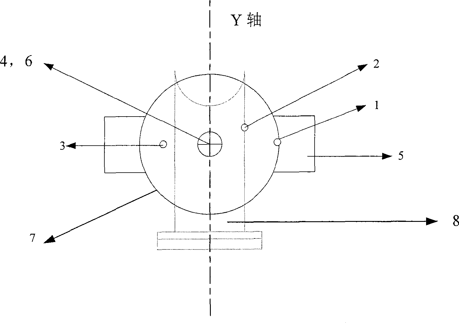
[0035] Such as figure 1 As shown, the substrate offset diagnosis and correction device of the present invention includes a diagnosis unit and a correction unit.

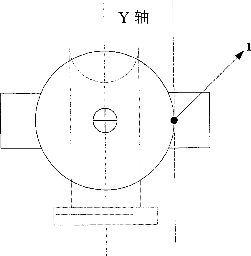
[0036] Such as figure 1 , 2 As shown, the diagnostic unit includes a first sensor 1, and the first sensor 1 is placed on the tangent line of the outer circumference of the substrate when the center 6 of the substrate coincides with the center 4 of the manipulator finger, wherein the tangent line is a tangent line parallel to the Y axis. In this embodiment, the first sensor 1 adopts a photoelectric sensor, including a light emitting device and a light receiving device, and the light emitting device and the light receiving device are respectively arranged above and above the plane where the substrate is located at a distance from the tangent position. below.

[0037] In fact, the above diagnostic unit alone can constitute a substrate offset diagnostic device.

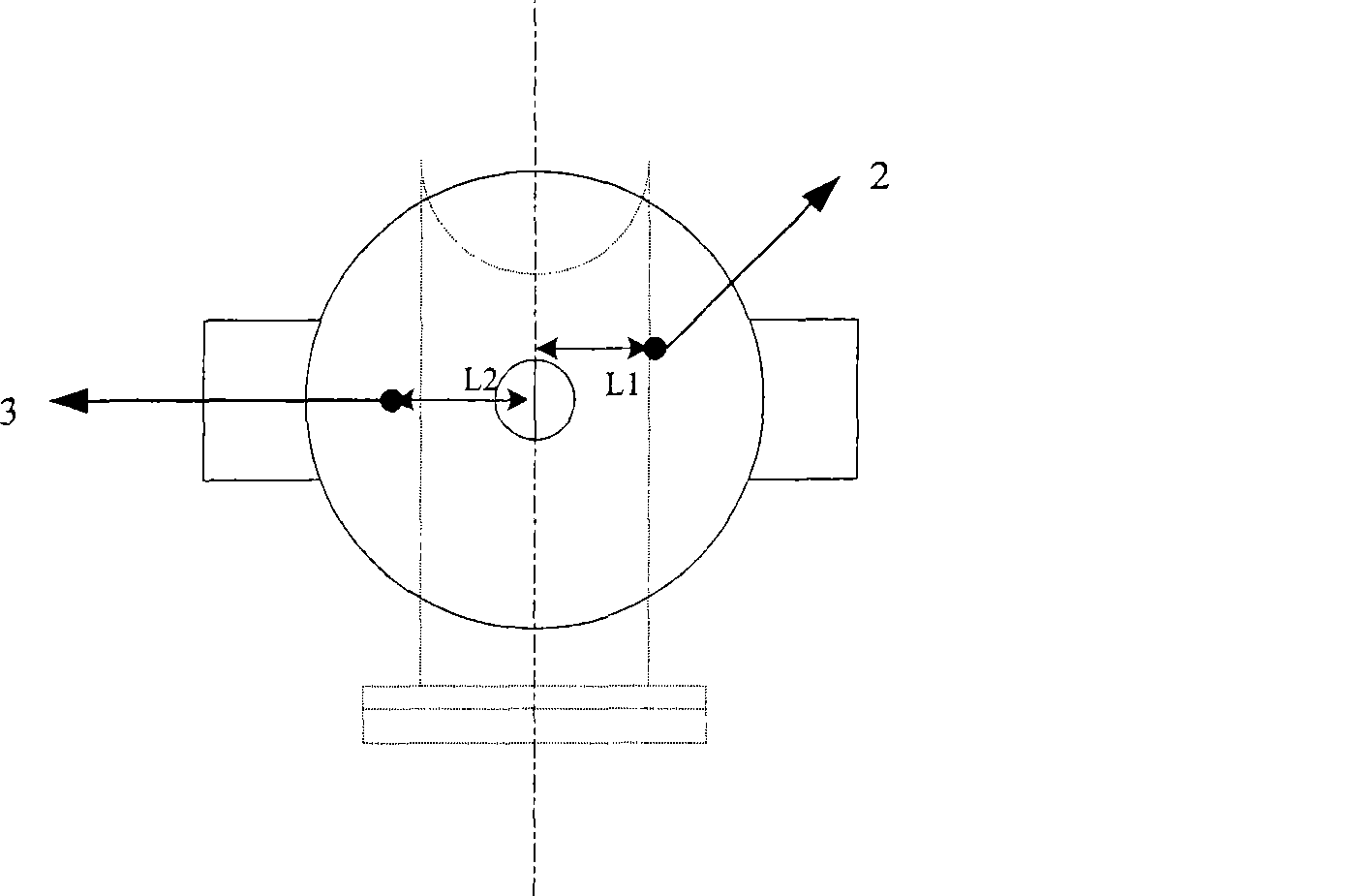
[0038] Such as figure 1 , 3 As shown, the calibratio...


PUM


Abstract

The invention discloses a substrate offset diagnosis and correction method, which comprises a diagnosis step (10) and a correction step (20) as follows: in the diagnosis step, determining whether the substrate carried by a transmission part is offset based on the detection result of a first sensor; in case of no offset, do not carry out the following correction step; in case of offset, carrying out the correction step; in the correction step, adjusting the location of the substrate, and then enabling the substrate to eliminate offset and return to the baseline position. In addition, the invention also provides a substrate offset diagnosis and correction device which comprises a diagnosis unit and a correction unit, wherein, the diagnosis unit is used to judge whether the substrate carried by the transmission part is offset; in case of offset, triggering the correction unit to work; in case of no offset, do not carry out any operation; the correction unit is used to adjust the location of the substrate and enable the substrate to eliminate offset and return to the baseline position. The method and the device are simple to use and enable the substrate to be accurately transmitted; besides, the device has high transmission accuracy and good reliability.

Description

technical field [0001] The present invention relates to the technical field of microelectronics, in particular to a method for diagnosing and correcting substrate offset, and also relates to a device for diagnosing and correcting substrate offset. Background technique [0002] In modern semiconductor substrate transfer, the central transfer chamber is surrounded by multiple process reaction chambers as the mainstream system architecture. The central transfer chamber is equipped with a vacuum robot to load and unload substrates for each reaction chamber surrounding the transfer chamber. piece. Processes including etching, physical and chemical vapor deposition, ion implantation, and photolithography can be performed in these reaction chambers. [0003] As feature sizes decrease and substrate sizes increase, the accuracy of substrate target position transfer around each reaction chamber becomes extremely important. High repeatability and accuracy of substrate transfer can en...

Claims


Application Information

Patent Timeline
IPC IPC(8): H01L21/68H01L21/66
Inventor 李永军
Owner 安徽尚特杰企业管理有限公司
Why Eureka
Try Eureka