Shower plate, method for manufacturing the shower plate, plasma processing apparatus using the shower plate, plasma processing method and electronic device manufacturing method

A plasma and processing device technology, applied in the field of plasma processing devices, can solve problems such as poor surface flatness, and achieve the effects of preventing electric field concentration, preventing ignition phenomenon, and preventing backflow

Inactive Publication Date: 2009-06-24
TOKYO ELECTRON LTD +1
View PDF4 Cites 4 Cited by
  • Summary
  • Abstract
  • Description
  • Claims
  • Application Information

AI Technical Summary

Problems solved by technology

However, since this structure also uses a general porous ceramic sintered body sintered at normal temperature and pressure, it cannot solve the above-mentioned problems caused by poor surface flatness.

Method used


Image

  • Shower plate, method for manufacturing the shower plate, plasma processing apparatus using the shower plate, plasma processing method and electronic device manufacturing method
  • Shower plate, method for manufacturing the shower plate, plasma processing apparatus using the shower plate, plasma processing method and electronic device manufacturing method
  • Shower plate, method for manufacturing the shower plate, plasma processing apparatus using the shower plate, plasma processing method and electronic device manufacturing method

Examples


Embodiment 1

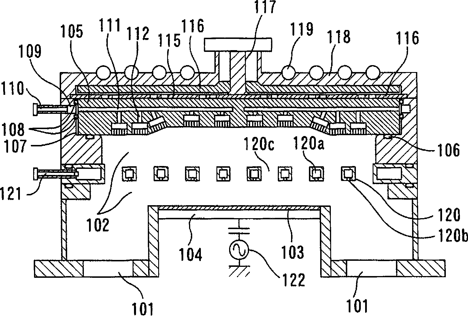
[0064] figure 1 Shows the first embodiment of the present invention. refer to figure 1 , represents a microwave plasma processing device. The illustrated microwave plasma processing apparatus has a processing chamber 102 exhausted through a plurality of exhaust ports 101 , and a holding table 104 for holding a substrate 103 to be processed is arranged in the processing chamber 102 . In order to exhaust the inside of the processing chamber 102 uniformly, the processing chamber 102 defines an annular space around the holding table 104, and a plurality of exhaust ports 101 are equally spaced in a manner communicating with the space, that is, relative to the substrate to be processed. 103 are arranged axially symmetrically. With the arrangement of the exhaust ports 101 , the processing chamber 102 can be uniformly exhausted from the exhaust ports 101 .

[0065] On the upper part of the processing chamber 102, an O-ring 106 for sealing is installed at a position corresponding...

Embodiment 2

[0099] Figure 5 Shows the second embodiment of the present invention. refer to Figure 5 , represents a microwave plasma processing device. The same reference numerals are assigned to the same reference numerals as those in the first embodiment, and description thereof will be omitted.

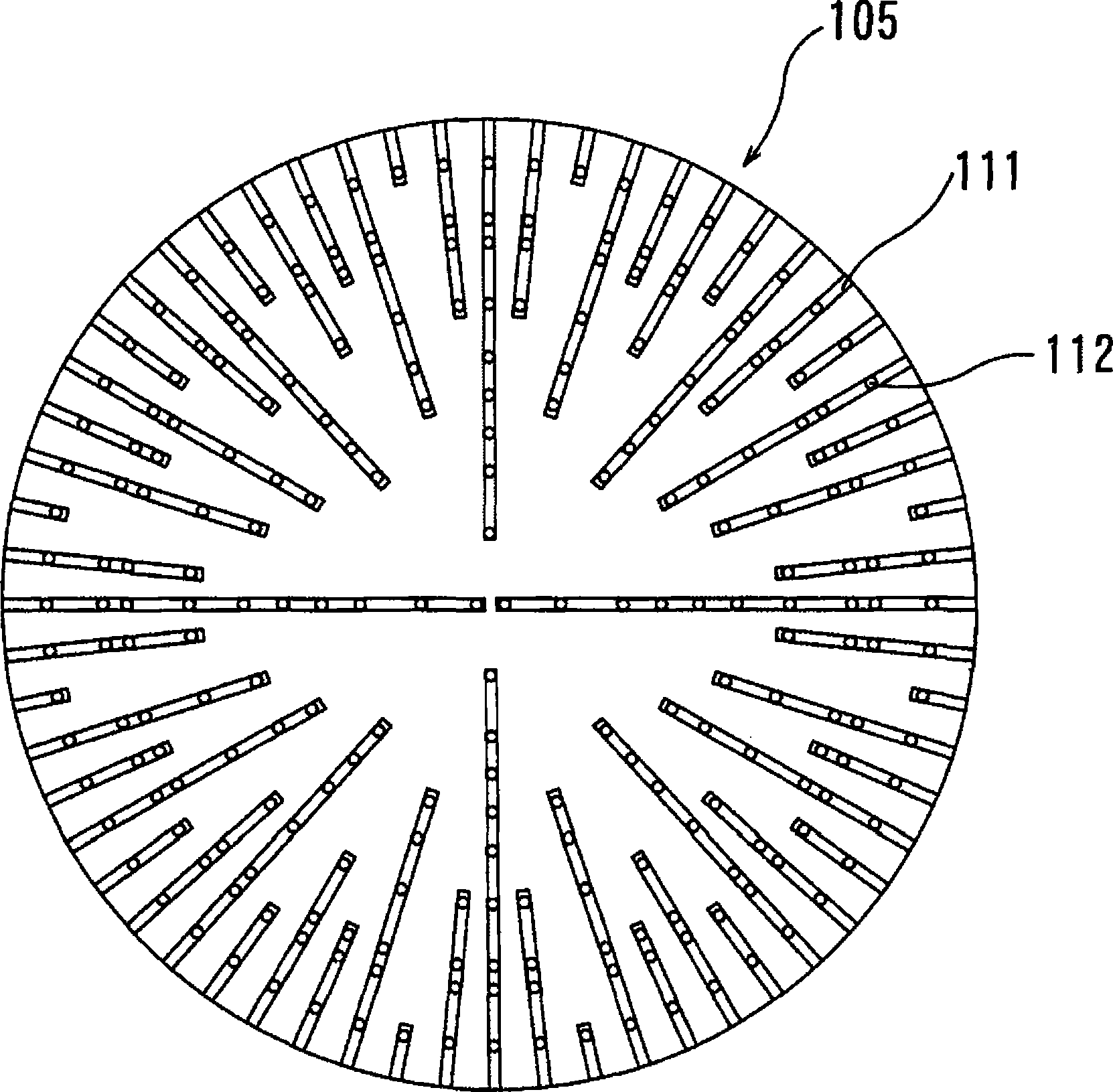
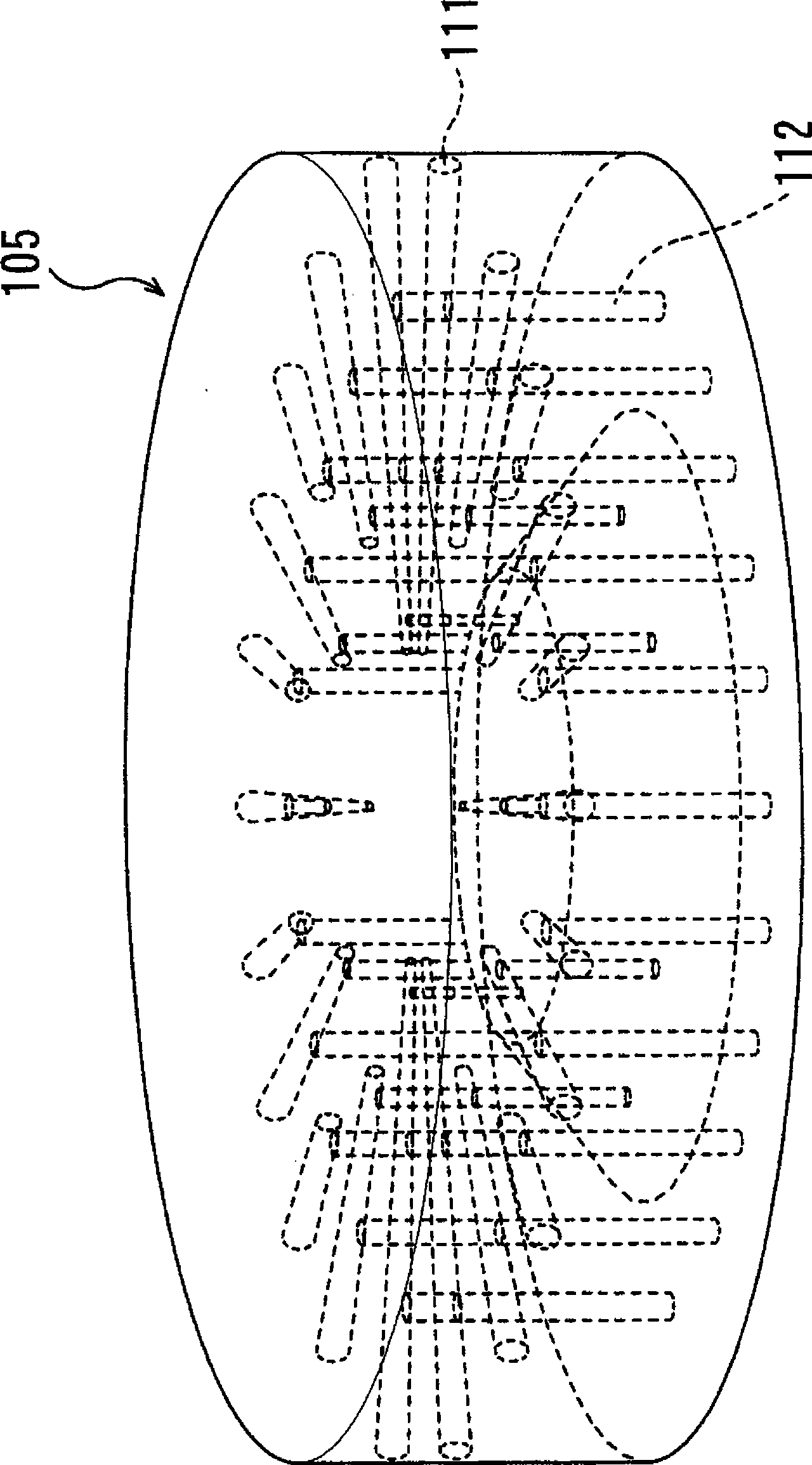
[0100] In this embodiment, an O-ring 106 for sealing is installed on the upper part of the processing chamber 102 as a part of the outer wall of the processing chamber 102 at a position corresponding to the substrate 103 to be processed on the holding table 104 as a relative medium. The electric constant is 9.8, and low microwave dielectric loss (dielectric loss is 1×10 -4 The plate-shaped shower plate 201 made of alumina and formed with a plurality of (230) openings, that is, vertical holes 200 , is a dielectric. And, in the processing chamber 102, an O-ring 203 for sealing is installed on the upper surface side of the shower plate 201, that is, on the opposite side to the holding table ...

Embodiment 3

[0110] Figure 10 A third embodiment of the present invention is shown. Referring to the figure, a microwave plasma processing apparatus is shown. The same reference numerals are assigned to the parts that overlap with those of the first and second embodiments, and description thereof will be omitted. The longitudinal hole 300 of the shower plate 301 in the present embodiment is Figure 11 construction shown. That is, a gas discharge hole 300a with a diameter of 0.05mm and a length of 0.5mm is opened on the side of the processing chamber 102 for exciting plasma, and the gas introduction side of the gas discharge hole 300a is connected to a hole 300b with a diameter of 1mm. In addition, in order to avoid electric field concentration of microwaves, chamfering 303 is performed on the corner portion of the hole 300 b on the gas introduction side. Then, a cylindrical porous ceramic sintered body 302 having a height of 5 mm and having pores communicating in the gas flow directio...


PUM

PropertyMeasurementUnit
diameteraaaaaaaaaa
bending strengthaaaaaaaaaa
diameteraaaaaaaaaa

Abstract

Provided is a shower plate which can completely prevent generation of plasma reverse flow or ignition of plasma excitation gas at a vertical hole section for more efficient plasma excitation. A shower plate (105) is arranged in a processing chamber (102) in a plasma processing apparatus, and discharges plasma excitation gas for generating plasma in the processing chamber (102). A porous gas communicating body (114) having pores communicating in a gas communicating direction is mounted on a vertical hole (112) to be a discharge path for the plasma excitation gas. The pore diameter of an overflow path in a gas communicating path formed by the communicating pores of the porous gas communicating body (114) is 10[mu]m or less.

Description

technical field [0001] The present invention relates to a shower plate used in a plasma processing device, especially a microwave plasma processing device, a method for manufacturing the same, a plasma processing device using the shower plate, a plasma processing method, and an electronic device. Manufacturing method. Background technique [0002] The plasma treatment process and the plasma treatment apparatus are essential for the manufacture of ultra-fine semiconductor devices with a gate length of 0.1 μm or less, which are called so-called deep submicron devices or deep sub-quarter micron devices in recent years. , is an indispensable technology for manufacturing high-resolution flat-panel display devices including liquid crystal display devices. [0003] Conventionally, various plasma excitation methods have been used as plasma processing apparatuses for manufacturing semiconductor devices and liquid crystal display devices, and in particular, parallel plate type high-f...

Claims


Application Information

Patent Timeline
Patent Type & Authority Applications(China)
IPC IPC(8): H05H1/46H01L21/205C23C16/455H01L21/3065
Inventor 桶作正广后藤哲也大见忠弘石桥清隆
Owner TOKYO ELECTRON LTD
Why Eureka
Try Eureka