Exposure apparatus

A technology of exposure device and exposure section, which is applied in the direction of exposure device of photoengraving process, exposure equipment of microlithography, cleaning and flexible articles, etc. The effect of shortening working time and long life

Active Publication Date: 2009-07-01
ORC MFG
View PDF2 Cites 15 Cited by
  • Summary
  • Abstract
  • Description
  • Claims
  • Application Information

AI Technical Summary

Problems solved by technology

Therefore, in the device described in Patent Document 1, the adhesive roller cannot always be brought into contact with the transfer roller.
Therefore, in this device, the transfer roller is arranged at a fix...

Method used


Image

  • Exposure apparatus
  • Exposure apparatus
  • Exposure apparatus

Examples


no. 2 approach

[0109]

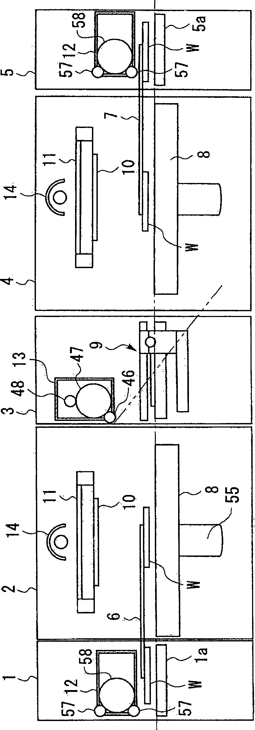
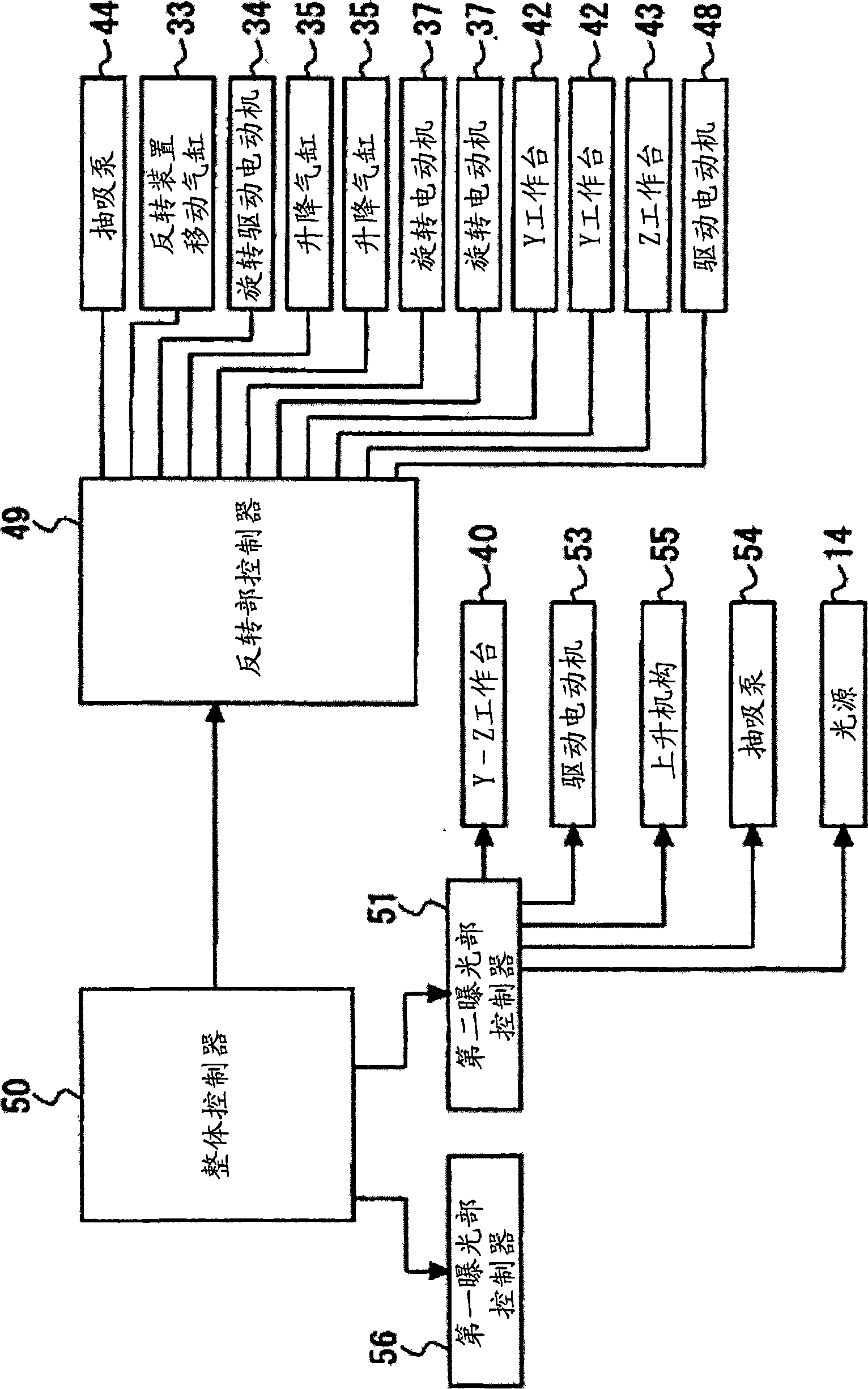
[0110] Figure 11 It is a side perspective view showing the overall structure of an exposure apparatus according to a second embodiment of the present invention. as it should Figure 11 As shown, compared with the exposure apparatus of the above-mentioned first embodiment, the second embodiment of the present invention only has the structure of the cleaning unit 21 in each exposure section 2, 4 and the control of each exposure section controller 51, 56 to Y- The Z stage 40 and the lifting mechanism 55 are different in the content of control, but the other structures are the same. Thus, in Figure 11 , for the same as in the first embodiment figure 1 The same elements of the structure shown are given with the figure 1 The same reference numerals are used, and explanations are omitted.

[0111]

[0112] The cleaning unit 21 of each exposure part 2, 4 of this embodiment is also supported by the YZ stage not shown, and moves so that a predetermined trajectory may...


PUM


Abstract

The present invention provides an exposure device which does not require complicated structure and can cause that the adhesion roller to contact with the transfer roller and simultaneously remove dust for the surface of objective table and the surface of workpiece. The adhesion rollers (57, 57) are projected and rotatablely supported pivotly on the side which is respectively opposite with the mask (10) and the objective table (8) to the cleaning unit (12) in each exposure part (2, 4). The peripheral surfaces of two adhesion rollers (57, 57) contact with the peripheral surface of large-diameter transfer roller (58) which is pivotly supported parallelly with the adhesion roller. Furthermore, a Y-Z objective table (40) causes that the adhesion roller (57) to contact with the mask (10) and remove dust for the surface of mask (10), so that the adhesion roller (57) contacts with the upper surface of objective table (8) and removes dust for the upper surface of objective table (8). Additionally, a reverting device (9) causes an adhesion base (30) to rotate around the rotation shaft. The adhesion base (30) exceeds a horizontal direction and stops at an inclined position. After the dust onthe surface of workpiece (W) is removed with a clearing unit (13), the adhesion base (30) is caused to face the horizontal direction.

Description

technical field [0001] The present invention relates to an exposure device for exposing a flat substrate on which a photoresist layer is formed on the surface of an electronic circuit substrate, a glass substrate for a liquid crystal element, a glass element substrate for a PDP (Plasma Display Panel, plasma display), etc. imaging. Background technique [0002] A photolithography method is used to form an image on a substrate such as an electronic circuit board (printed circuit board). The so-called photolithography is a method of forming a photoimage on the surface of a photoresist layer on a substrate, thereby selectively exposing the photoresist layer to light, and dissolving the photoresist layer by immersion in an etching treatment solution. , and then etch the substrate surface covered by the portion. In the photolithography method, as one of the methods of exposing the substrate, there is a contact exposure method in which a mask is overlapped with a surface to be ex...

Claims


Application Information

Patent Timeline
IPC IPC(8): G03F7/20H05K3/00B08B11/00
Inventor 屋木康彦水口信一郎石田肇松田政昭
Owner ORC MFG
Why Eureka
Try Eureka