
Duplexing touch control board

A touch panel and capacitive touch technology, applied in the field of receiving and processing devices, can solve the problems of low recognition rate, uneven refraction of image light on the display screen, and high product yield

Inactive Publication Date: 2009-07-01
YOUNG FAST OPTOELECTRONICS
View PDF0 Cites 16 Cited by
  • Summary
  • Abstract
  • Description
  • Claims
  • Application Information

AI Technical Summary

Problems solved by technology

[0003] The structure of the resistive touch panel mainly includes two transparent conductive films separated by a certain gap and arranged oppositely. The conductive film on the top is arranged on a surface of a flexible transparent film, and the conductive film on the bottom The film is set on one surface of a transparent glass substrate with a hard material, and the two conductive films are sealed in a board body; the upper and lower conductive films and the board body of this resistive touch panel are all transparent materials, so It is suitable to be configured in front of the display screen of electronic products, so that users can use the instructions on the screen to lightly touch and press the desired position of the panel to perform input functions, and it can be done by using commonly available pen tips and other objects Precise touch position operation, so it can be applied to smaller use area or higher-precision point input, especially suitable for input operations of character recognition with many strokes or complex shapes; however, the aforementioned resistive touch panel The input operation mode through the touch panel will cause the conductive film inside the board to withstand repeated stress and strain to cause damage, so the service life is limited, and when it is used for input with fingers or tools with thicker ends, it often gets relatively poor results. Inaccurate input results, so the adoption of input tools has many limitations
[0004] As for the structure of the capacitive touch panel, it slightly includes an x-axis sensing layer (x trace) and a y-axis sensing layer (y trace), so that the x-axis and y-axis sensing layers are insulated within the touch panel body, and the The x-axis and y-axis sensing layers are respectively grounded and connected to a control circuit. During operation, when a finger or conductor touches or lightly slides over the surface of the touch panel, a capacitive effect is generated at the moment the user's finger or conductor touches, Therefore, the control circuit can determine the touch position of the finger or the conductor through the change of the capacitance value; since the capacitive touch panel can be input by the finger, it has the convenience of input operation, and its input operation does not need to go through the touch pressure, so it will not let The panel has the disadvantage of being damaged by repeated stress and deformation, and this kind of touch panel has a simple structure, fewer components, high product yield, and is suitable for mass production to reduce costs; in addition, this kind of touch panel also has multi-point Sensing performance, which means that this kind of touch sensing device has the performance of multitasking control, so it can be used in high-level control operations, for example, in the control of video games, it can make the virtual subject being controlled more Actions are more flexible or have more diverse performances...; However, although the capacitive touchpad can be used for finger input, it is very convenient, but the accuracy of finger input sensing is not high, and it is easy to cause misoperation, resulting in use. It is troublesome, especially for the input of character recognition, such as Chinese characters with many strokes or complex shapes, the recognition rate is extremely low, and it is even difficult to reach a practical level, although the aforementioned problems can be solved by using a special However, it is still limited for use on a panel with a smaller area or for higher-precision point input. Moreover, the use of a special sensor pen often makes users feel very inconvenient in many occasions, such as When not carrying or losing pens
In addition, in recent years, some capacitive touch panels have changed to use light-transmitting insulating materials such as PET as the base material, and use low-impedance transparent conductive materials such as silver glue as the sensing layer to form a transparent capacitive touch panel. Control board, so it is suitable to be arranged in front of the display screen of electronic products, so that users can lightly touch and press the desired position of the panel through the instructions on the screen screen, and then perform function input; this existing transparent capacitor Type touch panel, the silver glue conductive material of the sensing layer is not completely transparent, and the sensing layers are respectively etched to form traces (Trace) of rhombus grid pattern, so that transparent traces are formed on the working area of ​​the touch panel. The stitched portion and the non-stitched portion (that is, the hollowed-out portion) with different light rates, because the stitched portion and the non-stitched portion with different light transmittances on the existing transparent capacitive touch panel are clearly separated, It will still cause uneven refraction of the image light on the display screen at the bottom of the transparent touch panel, resulting in blurred and distorted images

Method used


Image

  • Duplexing touch control board
  • Duplexing touch control board
  • Duplexing touch control board

Examples


Embodiment Construction

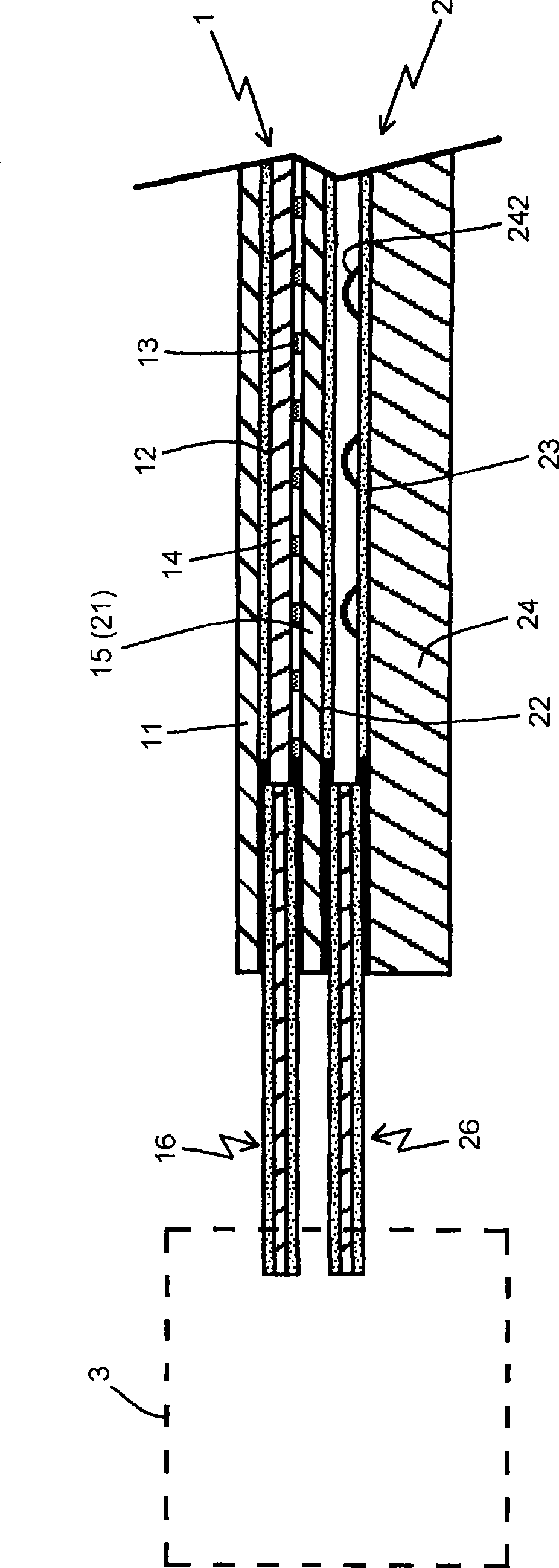
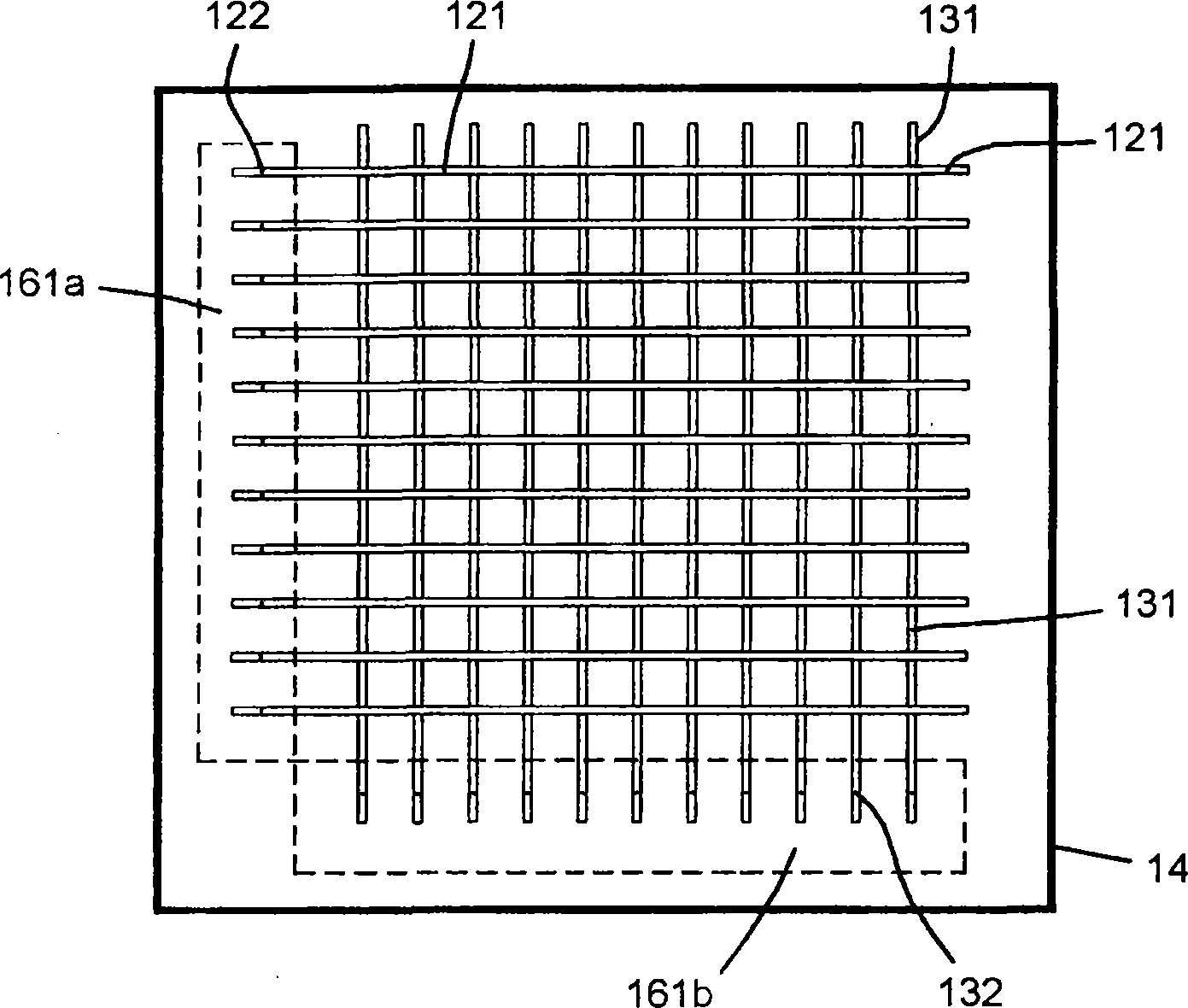
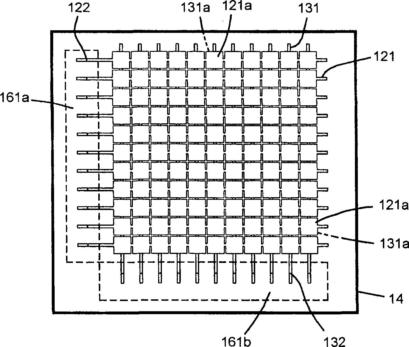
[0024] Such as Figure 1 to Figure 2Shown is a preferred embodiment of the present invention, which includes a capacitive touch panel unit 1, a resistive touch panel unit 2, and a signal processing unit 3; wherein, the capacitive touch panel unit 1 includes a surface Layer 11, X-axis sensing layer 12, Y-axis sensing layer 13, an insulating layer 14, a base layer 15, and a first signal output wiring 16; wherein, the surface layer 11 and the base layer 15 have a high light transmittance The insulating thin layer material is glass, polycarbonate (Polycarbonate, PC), polyester (Polythylene terephthalate, PET), polymethylmethacrylate (polymethylmethacrylate, PMMA) or cycloolefin copolymer (Cyclic Olefin) Copolymer) film material, and a hardening treatment (Hard coat) process is also applied on the upper surface of the surface layer 11 to enhance the hardness of the working surface to avoid easy scratches and wear; and the X-axis sensing layer 12 and the Y-axis sensing layer 13 can...


PUM

PropertyMeasurementUnit
Widthaaaaaaaaaa

Abstract

The invention relates to a duplex touch pad, which is spliced by combining a capacitance-type touch pad unit and a resistance-type touch pad unit to form a combined touch pad body, thereby enabling the combined touch pad to have a touch induction interface of the capacitance-type touch pad and the resistance-type touch pad. Touch induction signals of the two touch pad units of the combined touch pad are transmitted to a signal processing unit, the signal processing unit at least provided with one signal discrimination circuit discriminates types of touch induction signals transmitted by the capacitance-type touch pad unit and / or the resistance-type touch pad unit, automatically selects a suitable signal processing mode and non-interlaced signal processing steps. The capacitance-type touch pad unit is respectively provided with a plurality of transparent stitches which are equidistant and are arrayed parallelly at a first axial stitch and a second axial stitch, thereby enabling the first axial stitch and the second axial stitch to be perpendicularly intercrossed, separated from and opposite to each other. Expanded induction surfaces are respectively arranged on intercrossed junctions of the first axial stitch and the second axial stitch, thereby increasing the luminousness uniformity of the working area of the touch pad.

Description

technical field [0001] The invention relates to a duplex touch panel, in particular to a touch sensing interface equipped with both a capacitive touch panel and a resistive touch panel, and a device for receiving and processing touch sensing signals. Background technique [0002] The production technology of touch sensing devices used on the display screens of electronic products has matured in recent years. The performance and quality of related component products have been continuously improved, and the price has been greatly reduced. Touch sensing devices have been widely used in various electronic products; generally speaking, touch sensing devices can be roughly divided into three types: capacitive touch panels, resistive touch panels, and electromagnetic touch panels. Touch panels such as touch panels have their own functional characteristics and advantages and disadvantages, so the current development and application layers are also different. For example, resistive t...

Claims


Application Information

Patent Timeline
IPC IPC(8): G06F3/041G06F3/045
Inventor 杨恺悌
Owner YOUNG FAST OPTOELECTRONICS
Learn More