Method for making laminated travelling wave electroabsorption modulation laser with epitaxial selection region

A technology of selective area epitaxy and manufacturing method, which is applied in the field of manufacturing selective area epitaxial laminated traveling-wave electroabsorption modulation lasers, which can solve the problems of long production cycle, increased laser threshold current, complex process, etc., and achieves good far-field characteristics , small threshold current, huge competitive advantage

Inactive Publication Date: 2009-07-01
INST OF SEMICONDUCTORS - CHINESE ACAD OF SCI
View PDF0 Cites 15 Cited by
  • Summary
  • Abstract
  • Description
  • Claims
  • Application Information

AI Technical Summary

Problems solved by technology

Although the Butt-joint method can optimize the structure of the laser and the modulator separately and improve the overall performance of the device, this method requires multiple epitaxial growths, the process is complex, the production cycle is long, and the cost is high. The coupling between the laser and the modulator efficiency is not high
The SAG technology process is relatively simple, only one epitaxy is required for the active area, and the optical coupling efficiency is high, but it cannot optimize the active area structure of the laser and the modulator separately, and the function is difficult to perform satisfactorily
The dual-stack MQW method has a simple process, only one epitaxy is required for the active region, and the multiple quantum well (MQW) structures of the laser and the modulator can be optimized separately, but the performance of the active region of the laser is greatly affected by the stacking of the modulator in the vertical direction. Large, resulting in an increase in the threshold current of the laser, and a low light output power of the EML device

Method used


Image

  • Method for making laminated travelling wave electroabsorption modulation laser with epitaxial selection region
  • Method for making laminated travelling wave electroabsorption modulation laser with epitaxial selection region
  • Method for making laminated travelling wave electroabsorption modulation laser with epitaxial selection region

Examples


Embodiment Construction

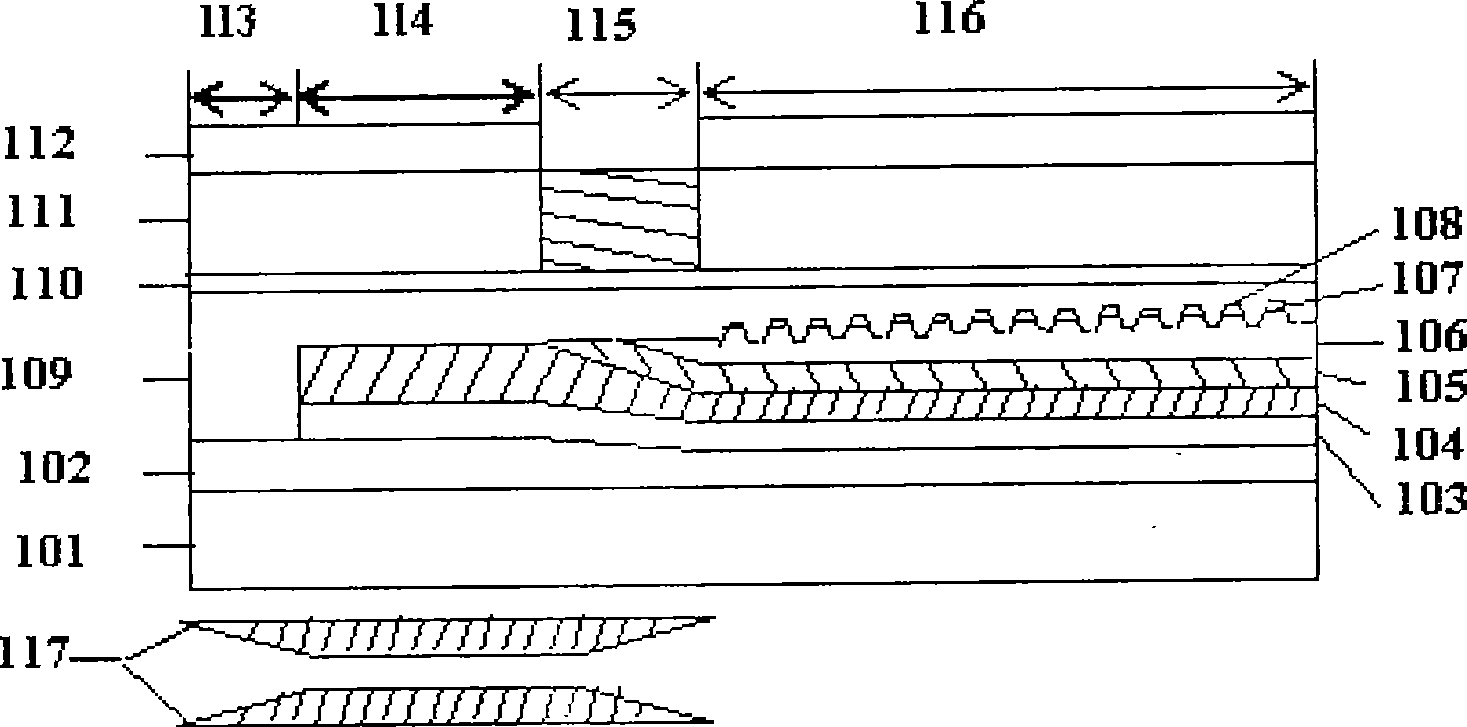
[0033] The process of fabricating a traveling-wave electroabsorption modulation laser with a stacked structure in an active region by the selective area epitaxy (SAG) technology of the present invention is described below with reference to the above-mentioned drawings.

[0034] figure 1For the longitudinal structural schematic diagram of the selective area epitaxy stacked traveling-wave electroabsorption modulation laser used in the present invention, first make a wedge-shaped dielectric mask strip pattern 117 on the semi-insulating InP substrate 101, and then epitaxially epitaxially on the semi-insulating InP substrate 1 grow heavily doped n-InP buffer layer 102, 1.2Q lower confinement layer 103, modulator MQW structure 104, laser MQW structure 105, 1.2Q upper confinement layer 106 and n-InP inversion layer 107; The upper stacked MQW structure 105 (MQW of DFB) in the stacked MQW structure in the regions 113-114, together with the lower stacked MQW structure 104 (MQW of EAM) a...


PUM


Abstract

The invention relates to the fabrication method of a travelling-wave electroabsorption modulated laser with a laminated structure formed by selective-area growth (SAG). The fabrication method comprises the following steps: fabricating a mask strip pattern on a semi-insulating InP substrate; sequentially epitaxially growing a heavily-doped n-InP buffer layer, a 1.2Q lower confinement layer, a multi-quantum well structure of a modulator, a multi-quantum well structure of a laser, a 1.2Q upper confinement layer and an n-InP inversion layer; etching off an upper laminated multi-quantum well structure in a SAG laminated multi-quantum well structure, and a lower laminated multi-quantum well structure and the 1.2Q lower confinement layer of an optical terminal region; fabricating a grating on a large-area growth area, and etching an inversion layer to the 1.2Q upper confinement layer by the grating; and sequentially epitaxially growing a p-InP protection layer, an etching stop layer, a p-InP cover layer and a p-InGaAs layer; and etching off the p-InGaAs layer in the electrical insolation area, and implanting ions in the p-InP cover layer in the area to produce a high-impedance area.

Description

technical field [0001] The invention relates to a method for manufacturing a traveling-wave electroabsorption modulation laser with a stacked structure in an active region by using a selective area epitaxy (SAG) technology. Background technique [0002] With the development of the information age, the existing communication network can no longer meet the requirements of communication capacity and speed, and many high-speed optoelectronic devices are competing to be developed. In the field of laser light sources for optical communications, traditional lumped electroabsorption modulation lasers are difficult to greatly improve the modulation bandwidth due to the limitation of their own structural characteristics. Traveling-wave electro-absorption modulated lasers are becoming the mainstream of laser light sources for communication because of their great potential for improvement in modulation bandwidth. [0003] One of the research focuses of traveling-wave electroabsorption ...

Claims


Application Information

Patent Timeline
Patent Type & Authority Applications(China)
IPC IPC(8): H01S5/343H01S5/22H01S5/06H01S5/00
Inventor 王桓朱洪亮潘教青程远兵
Owner INST OF SEMICONDUCTORS - CHINESE ACAD OF SCI
Why Eureka
Try Eureka