LED chip construction and manufacturing method thereof

A technology of light emitting diode and chip structure, which is applied to electrical components, circuits, semiconductor devices, etc., can solve the problems of low light extraction rate, low light extraction efficiency, increased production cost, etc. problem solving effect

Active Publication Date: 2009-07-22
EPILIGHT TECH +1
View PDF0 Cites 35 Cited by
  • Summary
  • Abstract
  • Description
  • Claims
  • Application Information

AI Technical Summary

Problems solved by technology

However, LEDs still have the problems of poor heat dissipation and low light output rate, because heat dissipation directly affects the reliability of LEDs, thereby affecting their life and applications, and low light output efficiency directly restricts the development of LEDs.
The current method to solve the heat dissipation problem of LEDs is mainly to add heat-conducting metal plates or

Method used


Image

  • LED chip construction and manufacturing method thereof
  • LED chip construction and manufacturing method thereof
  • LED chip construction and manufacturing method thereof

Examples


Embodiment Construction

[0027] The contents, advantages and objects of the present invention will be set forth in the following description of the embodiments.

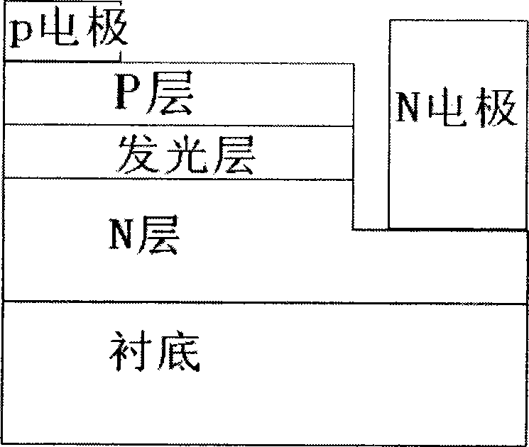
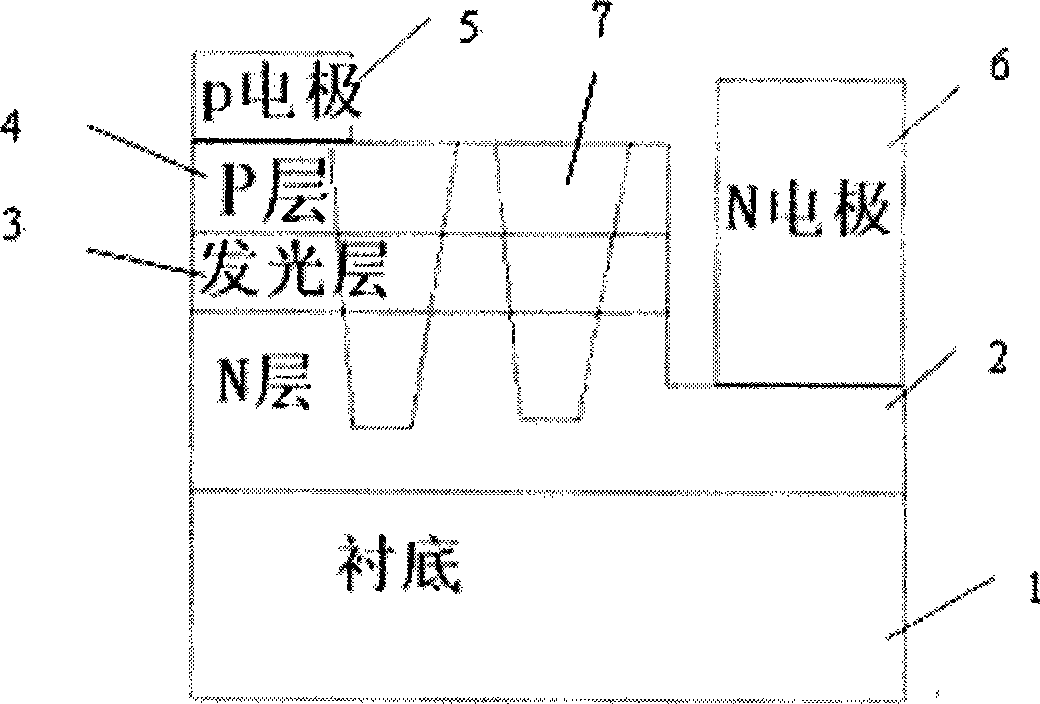
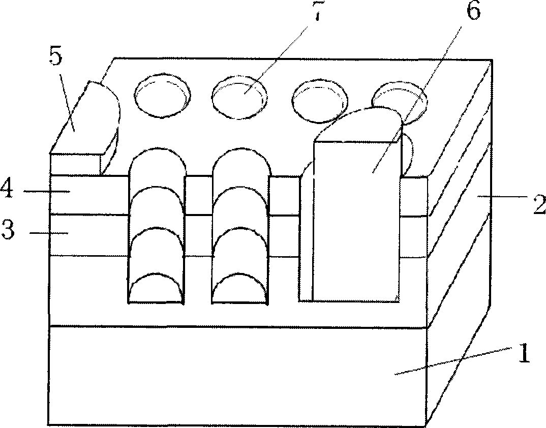
[0028] In the structural design of light-emitting chips, two problems urgently need to be solved are to provide good heat dissipation structure design and good current distribution to reduce chip temperature and improve light extraction efficiency. The present invention solves the above two problems at the same time through an ingenious structural design. On the premise of providing good heat dissipation, more light-emitting surfaces are provided so that light can be emitted from the side and the top surface at the same time. At the same time, due to the good current distribution design provided in both the P layer and the N layer, the current distribution is more uniform and reasonable. This kind of design can not only be used for general light-emitting chip design but also especially suitable for high-current power-type light-emitting diod...


PUM

PropertyMeasurementUnit
Apertureaaaaaaaaaa

Abstract

The invention provides a light emitting diode (LED) chip structure and a manufacture method thereof. Prior to manufacturing the traditional electrode structure, partial perforation is carried out on the well grown epitaxial structures by the method of wet etching or dry etching to cause the N-shaped gallium nitride layer to expose; meanwhile, the size and layout of the apertures are arranged reasonably according to the requirements of heat dissipation and current distribution. On the premise of ensuring good heat dissipation, the technical proposal provides more light-emitting surface so that light can be emitted from the lateral surface and the top surface simultaneously. At the same time, the current is distributed more evenly and reasonably owing to good current distribution design. The design not only can be used for common luminescence chips but also is especially suitable for power LED chip structures with high current. The technology mentioned in the invention fundamentally improves the heat dissipation and light emitting efficiency and the improved required technique is simple and efficient and does not need extra processing equipment and materials.

Description

technical field [0001] The invention relates to a light emitting diode, in particular to a structure of a light emitting diode chip used in a light emitting diode and a manufacturing method thereof. Background technique [0002] LED is the abbreviation of English light emitting diode (light emitting diode). Its basic structure is a piece of electroluminescent semiconductor material, which is placed on a shelf with leads, and then sealed with epoxy resin around it to protect the inner core wire. role, so the shock resistance of LED is good. The core part of a light-emitting diode is a wafer composed of a p-type semiconductor and an n-type semiconductor, and there is a transition layer between the p-type semiconductor and the n-type semiconductor, which is called a p-n junction. In the PN junction of some semiconductor materials, when the injected minority carriers recombine with the majority carriers, the excess energy will be released in the form of light, thereby directly ...

Claims


Application Information

Patent Timeline
IPC IPC(8): H01L33/00
Inventor 李淼刘善鹏颜建锋郝茂盛
Owner EPILIGHT TECH
Why Eureka
Try Eureka