Semiconductor device having insulated gate semiconductor element, and insulated gate bipolar transistor

A semiconductor and insulated gate technology, which is applied in the field of insulated gate bipolar transistors, can solve the problems that the device is prone to electromagnetic noise, the electric field distribution of the silicon substrate is uneven, and it is difficult to increase the breakdown voltage.

Active Publication Date: 2009-08-05
DENSO CORP +1
View PDF4 Cites 28 Cited by
  • Summary
  • Abstract
  • Description
  • Claims
  • Application Information

AI Technical Summary

Problems solved by technology

[0016] However, in Figure 29-34 In the trench IGBT shown in and the trench IGBT and IEGT disclosed in the above references, the breakdown voltage may be low
Alternatively, due to the hard switching nature of these devices, electromagnetic noise can easily be generated in the device
The reason why it is difficult to increase the breakdown voltage...

Method used


Image

  • Semiconductor device having insulated gate semiconductor element, and insulated gate bipolar transistor
  • Semiconductor device having insulated gate semiconductor element, and insulated gate bipolar transistor
  • Semiconductor device having insulated gate semiconductor element, and insulated gate bipolar transistor

Examples


no. 1 example

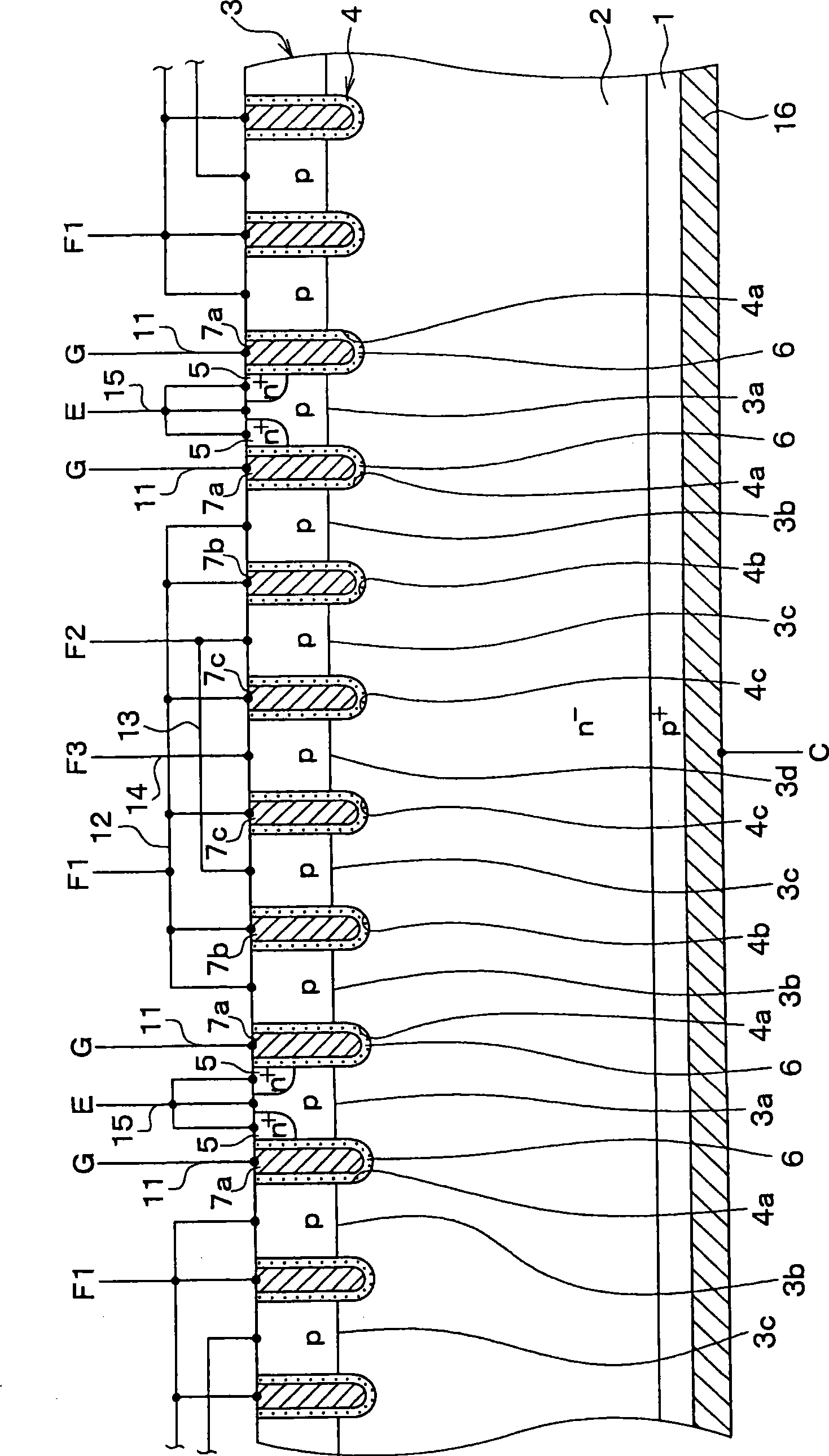
[0064] figure 1 shows along the image 3 A semiconductor device with an IGBT intercepted by the line I-I in . figure 2 shows along the image 3 The device intercepted by the line II-II. although image 3 Not a sectional view, but image 3 There are shaded areas in , to facilitate understanding of the structure.

[0065] In P with a major surface + The IGBT is formed in the substrate 1. Substrate 1 has a high impurity concentration. N is formed on the main surface of the substrate 1 by an epitaxial growth method - Type drift layer 2. Drift layer 2 has a lower impurity concentration than substrate 1 .

[0066] P-type base region 3 having a predetermined thickness is formed in a surface portion of drift layer 2 . A plurality of trenches 4 are formed on the substrate 1 such that each trench 4 penetrates the base region 3 and reaches the drift layer 2 . Base region 3 is divided into a plurality of base portions by trenches 4 . Specifically, grooves are provided at pr...

no. 2 example

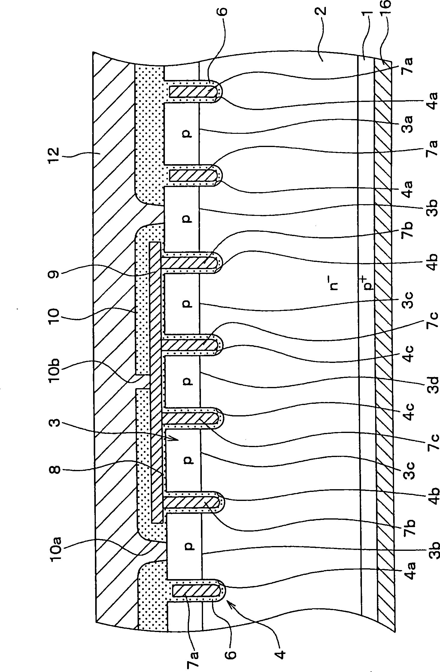
[0082] In the second embodiment, with Figure 1-4 The gate electrode 7a, the dummy gate electrodes 7b, 7c, and the first to third floating layers 3b-3d are connected to each other in a different manner compared to the device in .

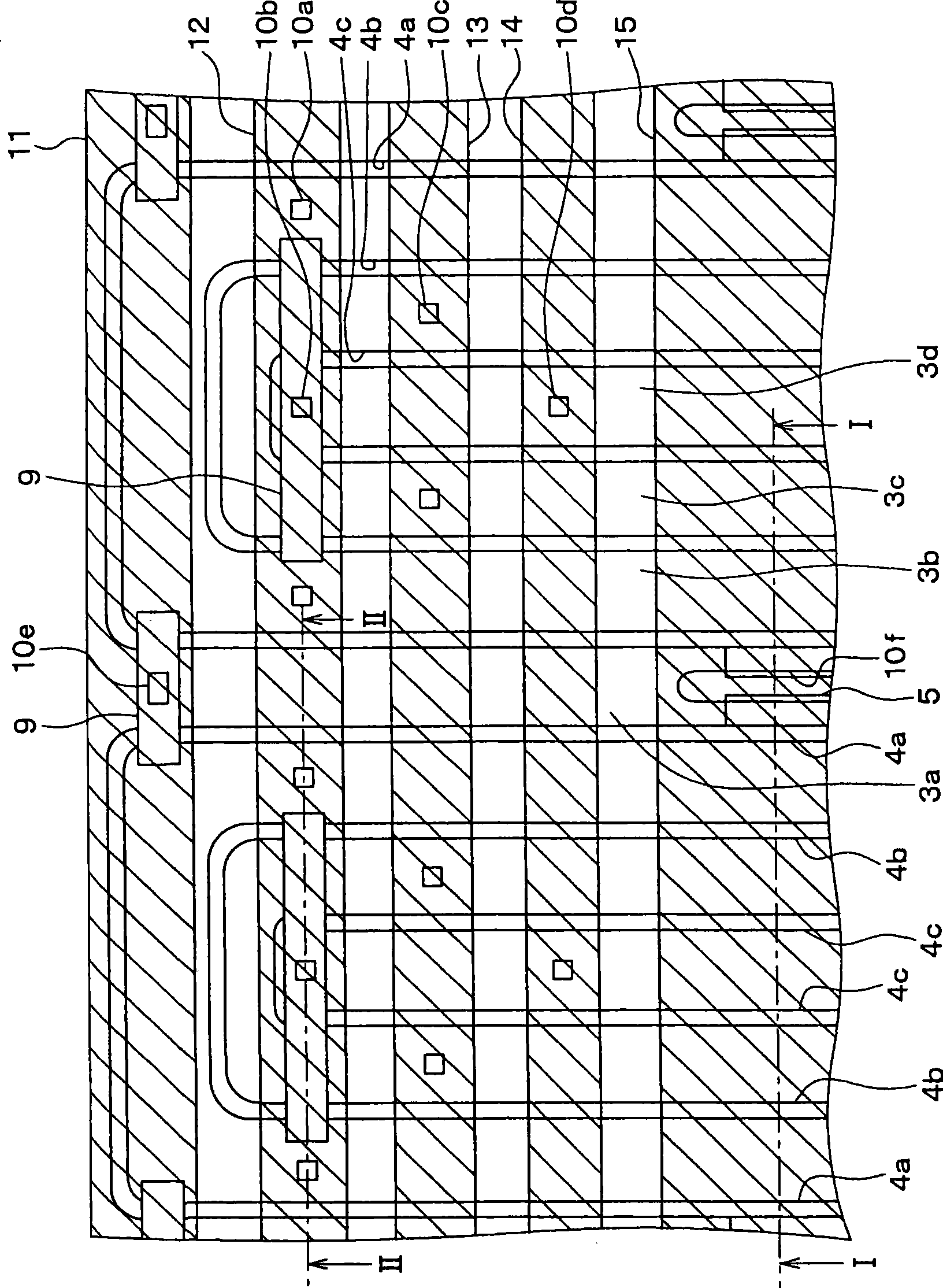
[0083] Figure 5 A semiconductor device according to the second embodiment is shown. Image 6 for along Figure 11 The cross-sectional view of the device taken at the line VI-VI, Figure 7 for along Figure 11 A cross-sectional view of the device taken along line VII-VII, Figure 8 for along Figure 11 A cross-sectional view of the device taken along the line VIII-VIII, Figure 9 for along Figure 11 The cross-sectional view of the device taken at line IX-IX, while Figure 10 for along Figure 11 A cross-sectional view of the device taken along line X-X in . Figure 11 Not a cross-sectional view, but in Figure 11 Shading is drawn in to facilitate understanding of the drawings.

[0084] Such as Figure 5 As shown, the dummy gate electro...

no. 3 example

[0089] In the semiconductor device according to the third embodiment, the arrangement of the gate wiring 11, the first to third floating wirings 12-14, and the emitter electrode 15 is different from that according to the first and second embodiments.

[0090] Figure 12 A semiconductor device having the IGBT according to the present embodiment is shown. Figure 12 Not a cross-sectional view, but in Figure 12 Shading is partially drawn in the middle to facilitate understanding of the drawings. The first to third floating wirings are provided on both sides of the emitter electrode 15 so that they sandwich the emitter electrode 15 . Further, the gate wiring 11 is provided on both sides of the emitter electrode 15 and on the first to third floating wirings 12 - 14 such that the gate wiring 11 sandwiches the emitter electrode 15 and the first to third floating wirings 12 -14. The device also includes a gate pad 11a for connecting the gate wiring 11 and an external circuit, a f...


PUM


Abstract

The invention discloses a semiconductor device with an insulated gate semiconductor component and an insulated gate bipolar transistor. A semiconductor device having an IGBT includes: a substrate; a drift layer and a base layer on the substrate; trenches penetrating the base layer to divide the base layer into base parts; an emitter region in one base part; a gate element in the trenches; an emitter electrode; and a collector electrode. The one base part provides a channel layer, and another base part provides a float layer having no emitter region. The gate element includes a gate electrode next to the channel layer and a dummy gate electrode next to the float layer. The float layer includes a first float layer adjacent to the channel layer and a second float layer apart from the channel layer. The dummy gate electrode and the first float layer are coupled with a first float wiring on the base layer. The dummy gate electrode is isolated from the second float layer.

Description

technical field [0001] The present invention relates to a semiconductor device having an insulated gate semiconductor element and an insulated gate bipolar transistor. Background technique [0002] Insulated gate semiconductor devices such as trench gate type transistors and IGBTs serve as high breakdown voltage insulated gate semiconductor devices having a trench gate structure. Figure 17 with 18 The IGBT disclosed in JP-A-2006-49455 is shown. Each IGBT includes an N + type emitter region 101 . A dummy trench 103 is formed in a region other than the emitter region 101 . Thus, a plurality of grooves are uniformly formed. Specifically, the emitter region 101 is not formed in the entire base region 102 but is formed in a part of the base region 102 . A trench 105 is formed in a portion of the base region 102 . A gate electrode 104 is formed in the trench 105 so that a gate voltage is applied to the gate electrode 104 . The emitter region 102 is not formed in another pa...

Claims


Application Information

Patent Timeline
IPC IPC(8): H01L27/082H01L23/535H01L29/72H01L29/40
CPCH01L2924/0002
Inventor 小山雅纪冈部好文浅井诚藤井岳志吉川功
Owner DENSO CORP
Why Eureka
Try Eureka