High power semiconductor device having a Schottky barrier diode

a technology of schottky barrier and semiconductor device, which is applied in the direction of semiconductor devices, diodes, electrical devices, etc., can solve the problems of easy latching up, easy damage of element, and easy occurrence of problems, so as to prevent damage to elements and/or miss operation, suppress parasitic effects, and prevent damage to elements

Inactive Publication Date: 2005-03-22
FUJI ELECTRIC CO LTD
View PDF6 Cites 18 Cited by
  • Summary
  • Abstract
  • Description
  • Claims
  • Application Information

AI Technical Summary

Benefits of technology

The semiconductor can be configured to suppress parasitic effects by forward biasing a PN junction capable of being biased in the forwards direction so that minority carriers are not generated, and by connecting a Schottky barrier diode, constituting a majority carrier device, in parallel with the PN junction. The Schottky barri

Problems solved by technology

However, in the case of an inductive load, if MOSFETs are employed having the complicated connection structure shown in FIG. 9, problems tend to arise due to parasitic effects.
When such a parasitic effect is produced by parasitic transistors, not only can element destruction oc

Method used


Image

  • High power semiconductor device having a Schottky barrier diode
  • High power semiconductor device having a Schottky barrier diode
  • High power semiconductor device having a Schottky barrier diode

Examples


first embodiment

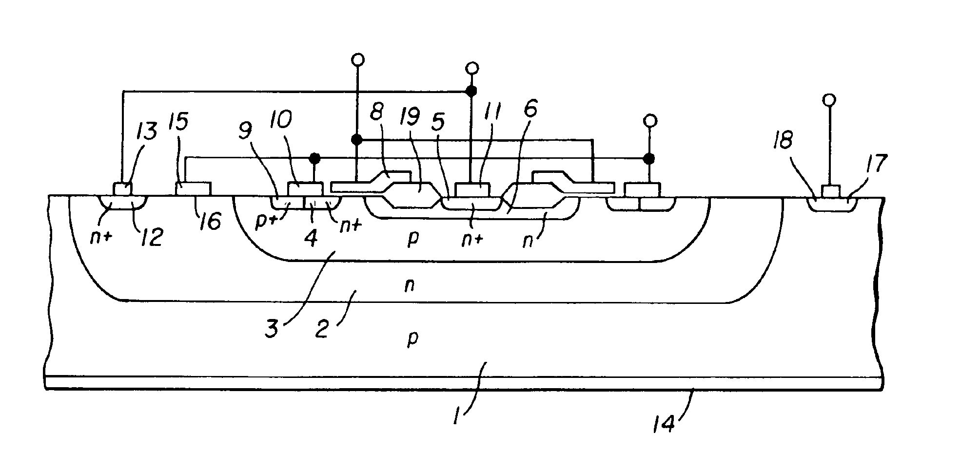
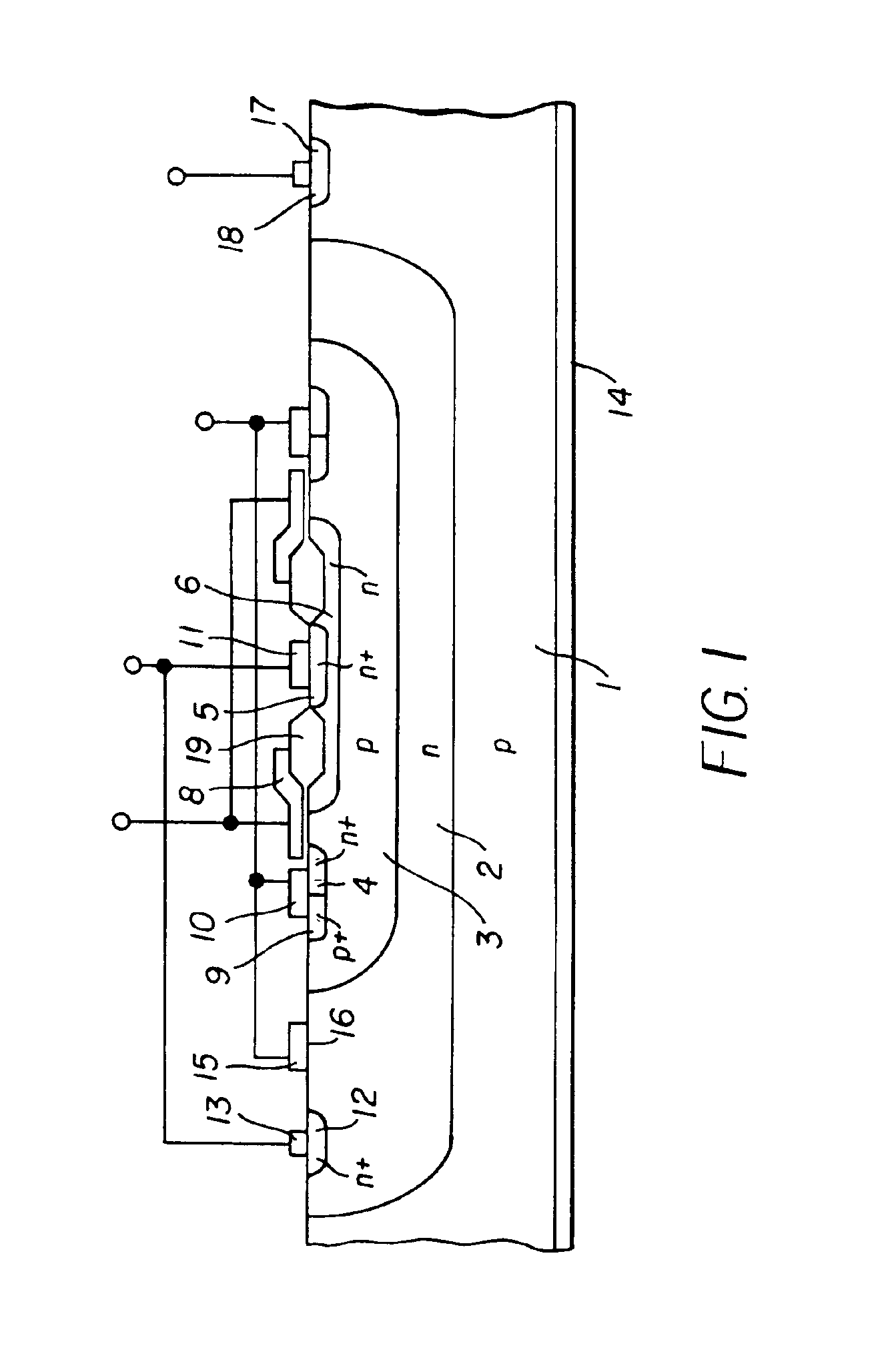
FIG. 1 is a cross-sectional constructional view illustrating the concept of a MOSFET incorporating a Schottky barrier diode according to the present invention. The difference between FIGS. 1 and 9 is that FIG. 1 has an anode electrode 15 formed at the surface of the n well region 2 and a Schottky junction 16 formed at the interface with the n well region 2. In this embodiment, the n well electrode 13 formed on the n+ contact region 12 is connected with the drain electrode 11 and the anode electrode 15 is connected with the source electrode 10, respectively, by means of wiring, so the Schottky barrier diode constituted by the anode electrode 15 and the n well region 2 is connected in parallel with the PN junction constituted by the p well region 3 and the drain region 5 (through the n offset region 6), so that the base current of the parasitic transistor is bypassed by the Schottky barrier diode, thereby making it possible to suppress the parasitic transistor effect. It should be not...

second embodiment

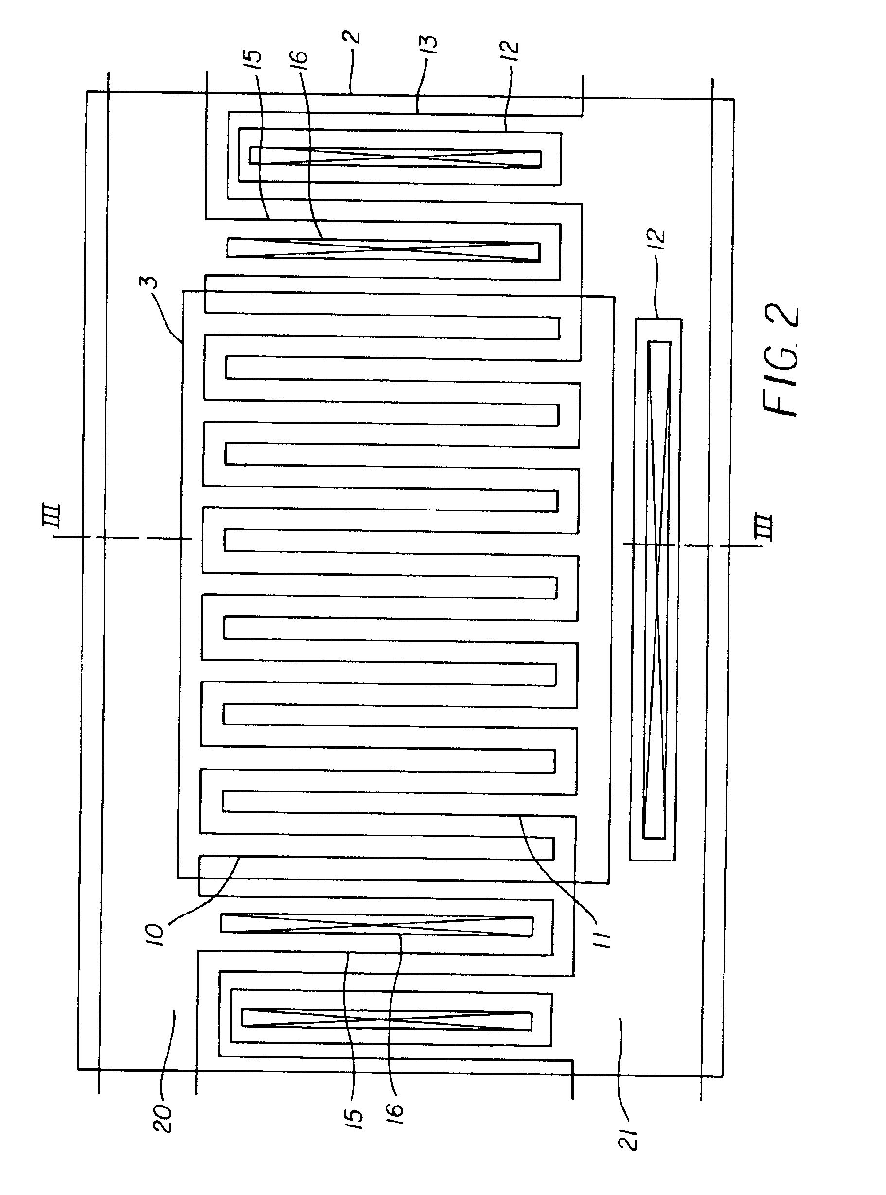
FIG. 4 is a plan constructional view of a MOSFET incorporating a Schottky barrier diode according to the present invention and FIG. 5 is a cross-sectional view along the line V—V of FIG. 4. The points of difference between this FIG. 4 and FIG. 5 with regard to FIG. 2 are that the Schottky junction 16 is formed directly below the region of the source current collector electrode 20 and that an n+ contact region 12a is provided in the vicinity of the source current collector electrode 20, being directly connected with the drain electrode at a tip portion thereof constituted by extending the drain electrode 11 from the drain current collector electrode 21. Since the source current collector electrode or drain current collector electrode must collect and allow passage of current from a large number of MOSFET cells, its wiring must be made comparatively wide. Consequently, if a Schottky barrier diode that requires a comparatively large area is formed in the region of such a source current...

fourth embodiment

FIG. 7 is a cross-sectional constructional view illustrating the concept of a Schottky barrier diode according to the present invention, in which an n well region 2 is formed at the surface of the p type semiconductor substrate 1 and, in addition, a p well region 3 is formed at the surface of the n well region 2. An n offset region 6 is formed at the surface of the p well region 3 and at the surface thereof there are formed an anode electrode 15 and cathode electrode 24, separated by a prescribed distance depending on the voltage-withstanding ability. The anode electrode 15 forms the n offset region 6 and the Schottky junction 16, and directly below the cathode electrode 24 there is formed an n+ cathode region 25 for forming an ohmic contact with the cathode electrode 24. Also, at the surface of the n offset region 6, which is sandwiched by the anode electrode 15 and cathode electrode 24, a LOCOS oxide film 19 and a polysilicon field plate 26 are formed with the object of moderating...


PUM


Abstract

A semiconductor device is configured to prevent destruction of elements and/or miss-operation of the circuit by parasitic effects produced by parasitic transistors when a MOSFET of a bridge circuit is formed on a single chip. A Schottky junction is formed by providing an anode electrode in an n well region where a source region, a drain region, and a p well region of a lateral MOSFET. A Schottky barrier diode constituting a majority carrier device is connected in parallel with a PN junction capable of being forward-biased so that the PN junction is not forward-biased so that minority carriers are not generated, and thereby suppressing parasitic effects.

Description

BACKGROUNDFIG. 10 is a cross-sectional constructional diagram of a MOSFET constituting a power semiconductor element employed in the output stage of a prior art intelligent switching device. In FIG. 10, an n well region 2 is formed at the surface of a p type semiconductor substrate 1 and a p well region 3 is formed at the surface of the n well region 2. An n+ source region 4 and n+ drain region 5 are formed at the surface of the p well region 3. In addition, a structure that moderates the electrical field of the PN junction between the n+ drain region 5 and p well region 3 is provided by forming an n offset region 6 of comparatively low concentration surrounding the n+ drain region 5. A gate electrode B is formed on the other side of a gate oxide film 7 at the surface of the p well region 3 that is sandwiched by the n+ source region 4 and the n offset region 6. A LOCOS oxide film 19 that is thicker than the gate oxide film 7 is formed at the edge of the gate electrode 8 on the drain...

Claims


Application Information

Patent Timeline
IPC IPC(8): H01L29/02H01L29/10H01L29/66H01L29/78H01L27/07H01L29/872H01L21/822H01L21/8234H01L27/02H01L27/04H01L27/06H01L27/088H01L29/47
CPCH01L27/0255H01L27/0727H01L29/7835H01L29/1087H01L29/47
Inventor KUMAGAI, NAOKIHARADA, YUUICHIJIMBO, SHINICHIIKURA, YOSHIHIROFUJIHIRA, TATSUHIKOYOSHIDA, KAZUHIKO
Owner FUJI ELECTRIC CO LTD
Why Eureka
Try Eureka