High-speed insulated gate bipolar transistor on lateral SOI

A bipolar transistor, insulated gate technology, applied in semiconductor devices, electrical components, circuits, etc., can solve the problems of slow turn-off time of lateral SOIIGBT, difficult to implement and manufacture, slow turn-off time, etc., to avoid auxiliary anode control circuit. , Increase the difficulty and cost of the process, and improve the effect of turning off the speed

Inactive Publication Date: 2010-07-07
UNIV OF ELECTRONIC SCI & TECH OF CHINA
View PDF0 Cites 20 Cited by
  • Summary
  • Abstract
  • Description
  • Claims
  • Application Information

AI Technical Summary

Problems solved by technology

The SOI IGBT with this structure has a better compromise between speed and on-resistance, but because an external circuit is required to apply a bias voltage to the anode auxiliary gate 12, and the bias voltage is a floating voltage, it is difficult to implement and manufacture
[0006] The above-mentioned lateral SOI

Method used


Image

  • High-speed insulated gate bipolar transistor on lateral SOI
  • High-speed insulated gate bipolar transistor on lateral SOI
  • High-speed insulated gate bipolar transistor on lateral SOI

Examples


Embodiment 1

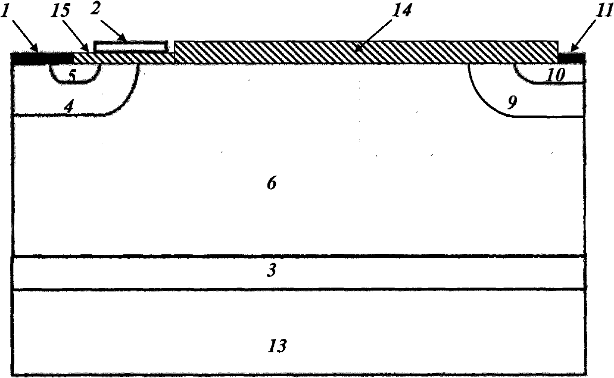
[0024] Embodiment 1: as Figure 4 , Figure 5 , Figure 6 and Figure 7 As shown, a high-speed lateral SOI insulated gate bipolar transistor, this embodiment is a non-punch-through (NPT, None-Punch-Through), including a substrate 13, a buried oxide layer 3, an N-base region 6, respectively located at the N The cathode region and the anode region at both ends of the base region 6 and the gate region above the cathode region are characterized in that the anode region is divided into a group of first anode region and second anode region by the isolation groove 8, and the first anode region An anode region includes P + anode region 10 and anode 11, the P + The anode region 10 is attached to the N base region 6, and the anode 11 is attached to the P + above the anode region 10; the second anode region includes the P drift region 7, the N + Anode region 17 and anode 11, the P drift region 7 and N + The anode region 17 is attached to the N base region 6, and the two ends of th...

Embodiment 2

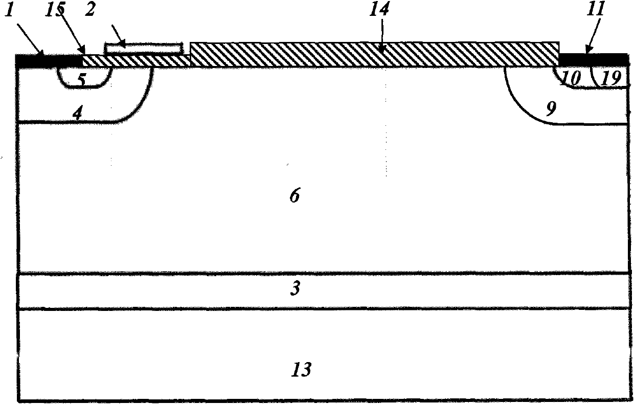
[0034] Embodiment 2: as Figure 8 , Figure 9 and Figure 10 As shown, a high-speed lateral SOI insulated gate bipolar transistor, this embodiment is a punch-through (PT, Punch-Through), this embodiment is based on the embodiment 1 in the N base region 6 of the first anode region and P + An N buffer zone 9 is added between the anodes 10, and the N buffer zone 9 is attached to the N base region 6, and the P + The anode region 10 is attached on the N buffer zone 9 and is separated from the N base region 6 . N buffer 9 to P + The hole injection from the anode 10 to the N-base region 6 has a regulating effect, so that the non-equilibrium carrier storage in the N-base region 6 is weakened, the device off-time is reduced, and the N buffer zone 9 can make the device block The withstand voltage structure of the device satisfies the RESURF condition, and under the same withstand voltage requirement, a shorter length of the N-base region 6 can be used.

[0035] In this embodiment,...


PUM


Abstract

The invention relates to a high-speed insulated gate bipolar transistor on a lateral SOI. The insulated gate bipolar transistor comprises a buried oxide layer, an N-based region, a cathode region and an anode region which are respectively arranged at the two ends of the N-based region and a gate region, field oxide and an anode field plate which are arranged above the cathode region, wherein the anode region is partitioned into at least one group of a first anode region and a second anode region by an isolation groove; the isolation groove isolates the P+ anode region of a first anode from the P drift region and the N+ anode region of a second anode; the isolation groove extends downwards to the buried oxide layer; and the field oxide layer is attached on the anode region, and the anode field plate is attached on the field oxide and is electrically connected with the anode of the anode region. The invention has the beneficial effects that: an on-resistance is not added while the turn-off speed of lateral SOI IGBT is improved, and the high-speed insulated gate bipolar transistor on the lateral SOI is provided.

Description

technical field [0001] The invention relates to semiconductor high-voltage devices in the field of electronic technology, in particular to conductance modulation high-voltage power devices manufactured on SOI (Silicon On Insulator, silicon on insulating layer). Background technique [0002] As a key component of SOI high-voltage integrated circuits, lateral SOI IGBTs (SOI Insulated Gate Bipolar Transistors) have the advantages of high current capability and easy integration, but their switching speed is much faster than that of lateral double-diffused metal oxide semiconductors. The field effect transistor (LDMOS, Lateral Double-diffused MOSFET) has a slow turn-off speed, and due to the current tail of the lateral SOI insulated gate bipolar transistor, its switching loss is large, which affects the lateral SOI insulated gate bipolar transistor. Applications of transistors in power integrated circuits. [0003] The conventional lateral SOI IGBT structure in the prior art is ...

Claims


Application Information

Patent Timeline
IPC IPC(8): H01L29/739H01L29/417H01L29/06
CPCH01L29/7394
Inventor 方健关旭陈文锁张波
Owner UNIV OF ELECTRONIC SCI & TECH OF CHINA
Why Eureka
Try Eureka