Thin SOI LIGBT device with carrier storage layer

A carrier storage and device technology, applied in semiconductor devices, electrical components, circuits, etc., can solve the problems of SOIL IGBT's small current capacity, reduced conductance modulation efficiency in the drift region, large forward conduction voltage drop, etc., and achieve fast turn-off Effects of speed, low turn-off loss, and low forward voltage drop

Active Publication Date: 2017-12-15
UNIV OF ELECTRONICS SCI & TECH OF CHINA +1
View PDF10 Cites 7 Cited by
  • Summary
  • Abstract
  • Description
  • Claims
  • Application Information

AI Technical Summary

Problems solved by technology

However, due to the presence of surface recombination that reduces the conductance modulation efficiency in the drift region, SOI LIGBTs with thin top silicon have problems of small current capability and large forward voltage drop.

Method used


Image

  • Thin SOI LIGBT device with carrier storage layer
  • Thin SOI LIGBT device with carrier storage layer
  • Thin SOI LIGBT device with carrier storage layer

Examples


Embodiment 1

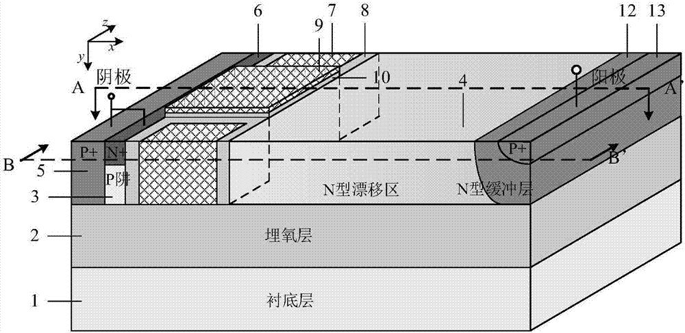
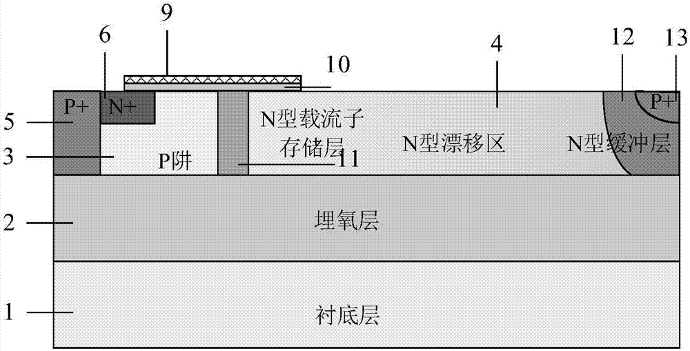
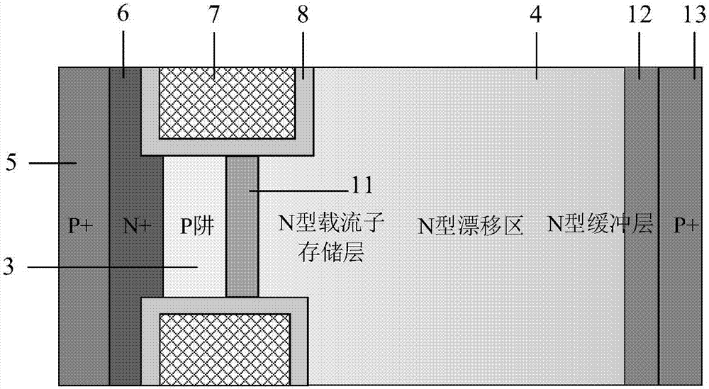
[0027] Such as figure 1 , 2 , 3, the thin SOI LIGBT device with the carrier storage layer of this example includes a substrate layer 1, a dielectric buried layer 2 and a top semiconductor layer that are sequentially stacked from bottom to top; along the lateral direction of the device, the The top semiconductor layer has a cathode structure, a trench gate structure, an N-type semiconductor drift region 4 and an anode structure in sequence from one side to the other;

[0028] The cathode structure includes a P-type well region 3 and a P-type heavily doped region 5 penetrating the top semiconductor layer along the vertical direction of the device, the P-type well region 3 and the P-type heavily doped region 5 are in contact with each other, and the P-type well region 3 is located at One side by the N-type semiconductor drift region 4; the upper layer of the P-type well region 3 has an N-type heavily doped region 6; the bottom of the P-type heavily doped region 5 and the P-type ...

Embodiment 2

[0037] Such as Figure 4 As shown, the difference between this example and Example 1 is that this example has a P-type layer 14 penetrating the top semiconductor layer along the vertical direction of the device on the side of the groove gate close to the N-type semiconductor drift region 4; Discontinuous distribution, the lengths of the two P-type layers 14 in the longitudinal direction are greater than or equal to the length of the corresponding groove grids in the longitudinal direction, and there is a distance between the P-type layers 14; The blocking effect of the carrier storage layer on the holes reduces the forward voltage drop; in the case of forward blocking, this example uses the depletion pinch-off effect of the P-type layer on the side of the trench gate close to the drift region on the drift region Realize normal withstand voltage; compared with embodiment 1, the doping concentration of the carrier storage layer in this example can be further increased, so that t...

Embodiment 3

[0039] Such as Figure 5 with 6 As shown, the difference between this example and Embodiments 1 and 2 is that, in this example, the planar gate structure and the grooved gates located on both sides of the planar gate structure along the device longitudinal direction constitute a three-gate structure. pole; such a gate connection method, the channel area becomes larger, the saturation current of the device increases, and the forward conduction voltage drop is reduced; compared with Examples 1 and 2, this example determines the position of the gate.


PUM


Abstract

The invention belongs to the technical field of power semiconductors, and specifically relates to a thin SOI LIGBT device with a carrier storage layer. The device is mainly characterized in that the device employs two trench gates and one plane gate structure, and the carrier storage layer is introduced between the two trench gates and below a plane gate. During forwarding conduction, the side walls of the trench gates block a hole loop, thereby achieving an effect of injection enhancement, and reducing the forwarding conduction voltage drop of a device. Meanwhile, the N-type carrier storage layer plays a role in hole blocking, promotes the electrons to be injected into a drift region, improves the electric conduction modulation effect, and further reduces the forwarding conduction voltage drop. During forwarding blocking, the trench gates play a role in using up the carrier storage layer, and enable the device to maintain a high withstand voltage under the high density of the storage layer. The beneficial effects of the invention are that the device, compared with a conventional LIGBT structure, is lower in forwarding conduction voltage drop, is higher in switching-off speed, and is lower in switching-off loss.

Description

technical field [0001] The invention belongs to the technical field of power semiconductors, and relates to a thin SOI LIGBT (Lateral Insulated Gate Bipolar Transistor, lateral insulated gate bipolar transistor) with a carrier storage layer. Background technique [0002] LIGBT is a hybrid structure composed of lateral field effect transistors and bipolar transistors. It combines the advantages of high input impedance and simple driving of MOSFETs, and the advantages of high current density and low turn-on voltage drop of BJT devices. One of the core electronic components in modern power electronic circuit applications. SOI LIGBT is compatible with standard CMOS circuits and is widely used in high-voltage integrated circuits. One such application is in a three-phase monolithic integrated inverter for driving a brushless DC motor. [0003] Researchers have done a lot of work, but these works mainly focus on thick top silicon, and pay less attention to thin top silicon. Comp...

Claims


Application Information

Patent Timeline
Patent Type & Authority Applications(China)
IPC IPC(8): H01L29/739H01L29/423H01L29/06
CPCH01L29/0603H01L29/42356H01L29/4236H01L29/7394
Inventor 罗小蓉杨洋孙涛魏杰邓高强黄琳华刘庆赵哲言曹厚华孙燕
Owner UNIV OF ELECTRONICS SCI & TECH OF CHINA
Why Eureka
Try Eureka