Gate voltage bootstrap sampling switch circuit adopting mirror image structure

A sampling switch and gate voltage bootstrap technology, applied in the field of microelectronics, can solve the problems affecting the linearity of the on-resistance of the MOS sampling switch, slowing down the speed, etc.

Active Publication Date: 2019-12-31
CHONGQING UNIV OF POSTS & TELECOMM
View PDF14 Cites 6 Cited by
  • Summary
  • Abstract
  • Description
  • Claims
  • Application Information

AI Technical Summary

Problems solved by technology

Thus, charge sharing affects the linearity of the on-resistance of the MOS sampling switch
At the same time, at the beginning of sampling, the MOS transistor M7 is turned on for a certain period of time before the MOS transistor M9 is turned on, which slows down the speed of the traditional grid voltage bootstrap sampling switch.

Method used


Image

  • Gate voltage bootstrap sampling switch circuit adopting mirror image structure
  • Gate voltage bootstrap sampling switch circuit adopting mirror image structure
  • Gate voltage bootstrap sampling switch circuit adopting mirror image structure

Examples


Embodiment

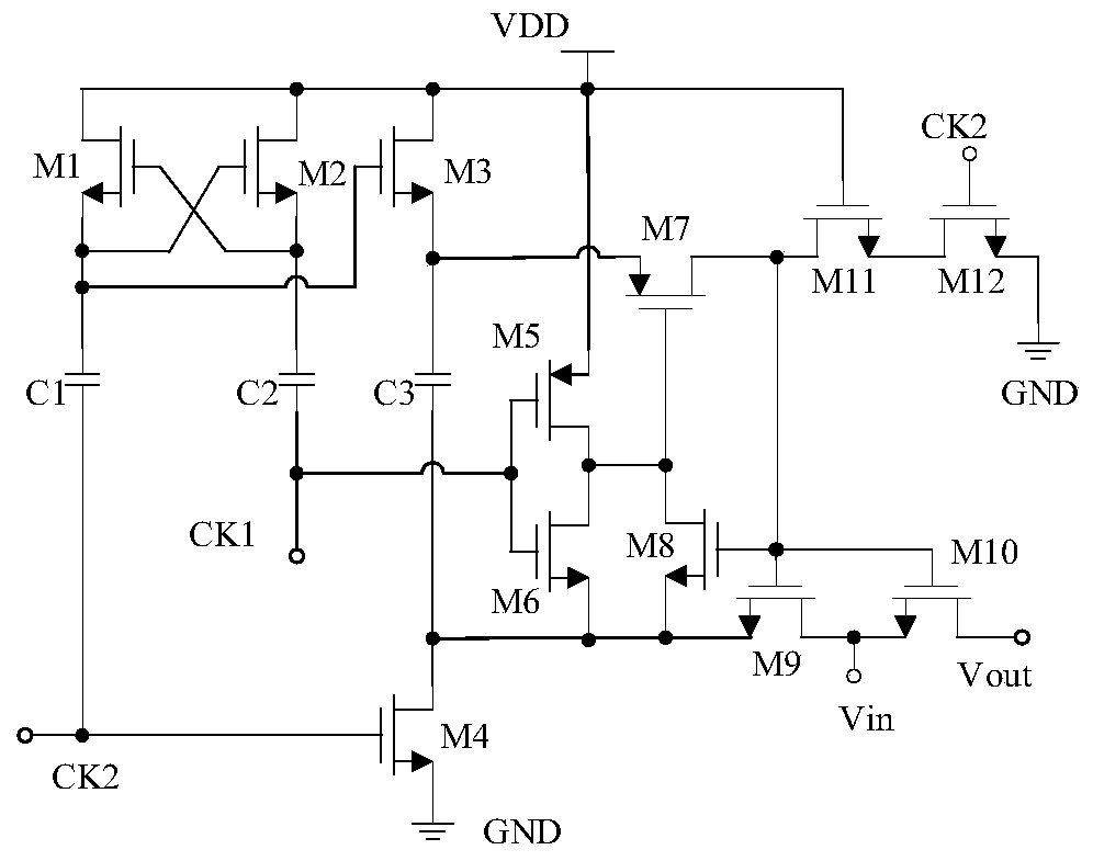
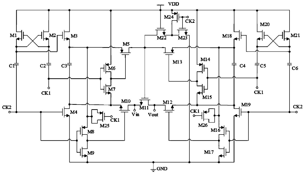
[0026] A mirrored gate voltage bootstrap sampling switch circuit, such as figure 2 As shown, it mainly includes: NMOS tube M1, NMOS tube M2, NMOS tube M3, NMOS tube M4, PMOS tube M5, PMOS tube M6, NMOS tube M7, PMOS tube M8, NMOS tube M9, NMOS tube M10, NMOS tube M11, NMOS tube M12, PMOS tube M13, PMOS tube M14, NMOS tube M15, PMOS tube M16, NMOS tube M17, NMOS tube M18, NMOS tube M19, NMOS tube M20, NMOS tube M21, NMOS tube M22, NMOS tube M23, PMOS tube M24, PMOS tube M25, PMOS tube M26, capacitor C1, capacitor C2, capacitor C3, capacitor C4, capacitor C5 and capacitor C6;

[0027] Wherein, the drain of the NMOS transistor M1 and the drain of the NMOS transistor M2, the drain of the NMOS transistor M3, the source of the PMOS transistor M6, the gate of the NMOS transistor M22, the source of the PMOS transistor M24, and the source of the PMOS transistor M14 , the drain of the NMOS transistor M18, the drain of the NMOS transistor M20, the drain of the NMOS transistor M21 are c...


PUM


Abstract

According to the gate voltage bootstrap sampling switch circuit adopting the mirror image structure, the bootstrap capacitance is increased to two times of that of a traditional circuit by adopting the mirror image structure, and the linearity of a sampling switch is improved; channel charge injection is inhibited by adopting a technology of absorbing channel charges generated by related MOS tubesby a clock-controlled virtual MOS tube; and a structure that the output end of a clock-controlled inverter drives an NMOS tube M10 and an NMOS tube M12 is adopted. The parasitic capacitance of the grid node of the sampling switch tube M11 is reduced; circuit charge sharing is suppressed, and, at the sampling start phase, the NMOS tube M10 and the NMOS tube M12 are respectively conducted with thePMOS tube MOS tube M5 and the PMOS tube M13 at the same time, and the conducted speed of the sampling switch is speeded up; and at the moment from sampling to holding conversion, a circuit composed ofthe PMOS tube M8 and the NMOS tube M9 and a circuit composed of the PMOS tube M16 and the NMOS tube M17 are kept on for a period of time at the same time, and the turn-off speed of the sampling switch is increased. According to the circuit, the linearity and the switching speed of the gate voltage bootstrap sampling switch circuit are effectively improved, so that the overall performance of the gate voltage bootstrap sampling switch circuit is effectively improved.

Description

technical field [0001] The invention belongs to the technical field of microelectronics, and in particular relates to a gate voltage bootstrap sampling switch circuit. Background technique [0002] With the development of integrated circuits, the Analog-to-digital Converter (Analog-to-digital Converter, ADC), as one of the main modules of the mixed-signal application system, is developing towards high speed and high precision. The sampling / holding circuit is the core circuit of the ADC, and the sampling switch is an important part of the sampling / holding circuit. Therefore, the performance characteristics of the sampling switch largely determine the performance characteristics of the sampling / holding circuit, which in turn determines the performance characteristics of the ADC. Therefore, the sampling switch undoubtedly becomes one of the important circuits of the ADC. [0003] figure 1 It is a traditional grid voltage bootstrap sampling switch, in which the MOS tube M10 is...

Claims


Application Information

Patent Timeline
Patent Type & Authority Applications(China)
IPC IPC(8): H03K17/042
CPCH03K17/04206
Inventor 周前能高唱李红娟
Owner CHONGQING UNIV OF POSTS & TELECOMM
Why Eureka
Try Eureka