Insulated gate bipolar transistor and method for producing same

A technology of bipolar transistors and insulated gates, which is used in semiconductor/solid-state device manufacturing, semiconductor devices, electrical components, etc., can solve problems such as poor improvement effect and failure to greatly improve switching speed, so as to improve circuit efficiency and enhance recombination probability. Effect

Inactive Publication Date: 2010-06-23
商海涵
View PDF4 Cites 20 Cited by
  • Summary
  • Abstract
  • Description
  • Claims
  • Application Information

AI Technical Summary

Problems solved by technology

[0003] Usually insulated gate bipolar transistors use field stop (fieldstop) technology to reduce on-resistance to improve their performance. The existing field stop technology of insulated gate bipolar transistors uses a slowly changing n+-Si layer as a...

Method used


Image

  • Insulated gate bipolar transistor and method for producing same
  • Insulated gate bipolar transistor and method for producing same
  • Insulated gate bipolar transistor and method for producing same

Examples


Embodiment Construction

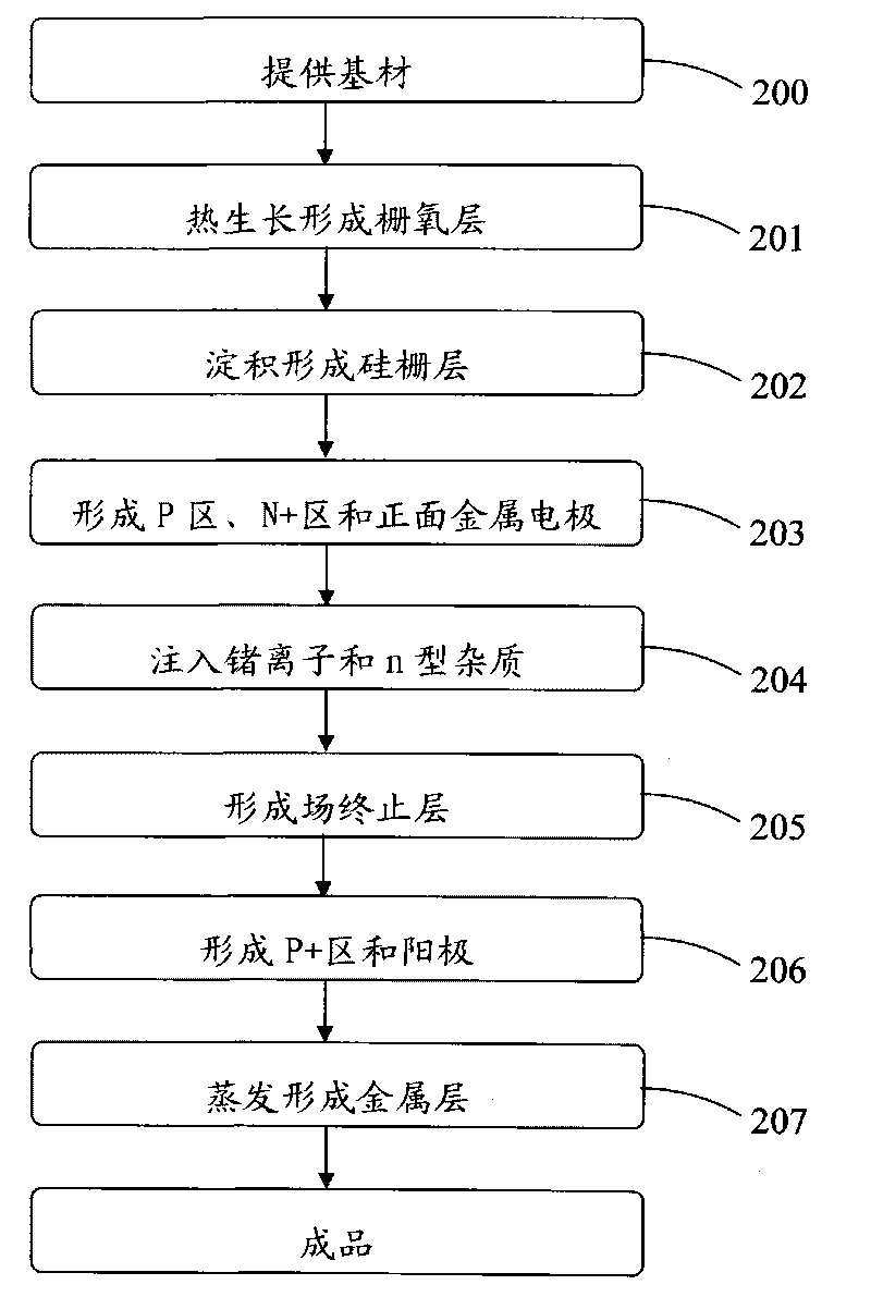
[0017] Below in conjunction with accompanying drawing and specific embodiment the present invention is described in further detail:

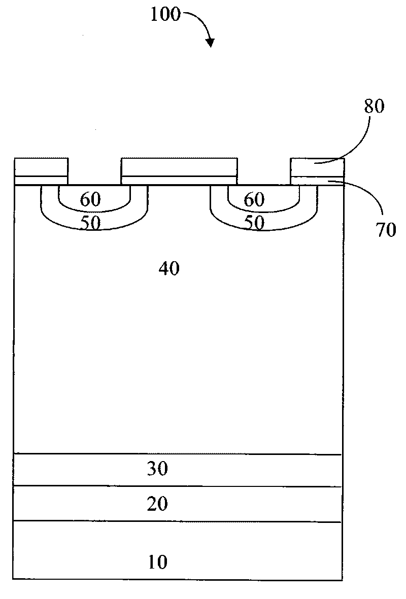
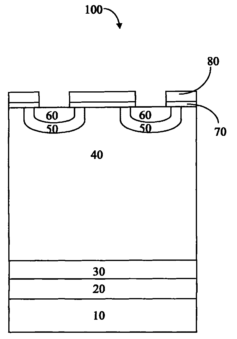
[0018] see figure 1 , is a schematic structural diagram of an insulated gate bipolar transistor 100 (Insulated Gate Biplar Transistor, IGBT) according to an embodiment of the present invention.

[0019] In this embodiment, the IGBT 100 is made of a silicon wafer, which includes a metal layer 10, a P+ region 20, a field stop layer 30, an N-region 40, a P region 50, an N+ region 60, a gate oxide layer 70 and a silicon gate layer 80, wherein the N-region 40 is a region fused silicon substrate, and the P+ region 20 is a P+ layer formed after boron implantation on the back side. The P region 50 and the N+ region 60 are located on the front side of the silicon wafer, and the P+ region 20 and the field stop layer 30 are located on the back side of the silicon wafer. The field stop layer 30 is located between the P+ region 20 and the N− region 40 and ...


PUM


Abstract

The invention provides an insulated gate bipolar transistor comprises a metal layer, a P+ area, a field termination layer, an N- area, a P area, an N+ area, a gate oxide layer and a silicon gate layer. The field termination layer comprises N-type silicon germanium alloy. The invention also provides a method for producing the insulated gate bipolar transistor. The insulated gate bipolar transistor uses the field termination layer of the N-type silicon germanium alloy as a reverse breakdown termination layer, thus the excess minority carrier hole recombination probability is enhanced, the turn-off time of the insulated gate bipolar transistor is shortened, the turn-off speed of the insulated gate bipolar transistor is increased and further the circuit efficiency is improved.

Description

technical field [0001] The invention relates to the field of manufacturing semiconductor power devices, in particular to an insulated gate bipolar transistor (Insulated Gate Biplar Transistor, IGBT) and a manufacturing method thereof. Background technique [0002] An insulated gate bipolar transistor (Insulated Gate Biplar Transistor, IGBT) is a voltage-controlled composite device composed of a MOSFET and a bipolar transistor. It combines the advantages of both devices, the characteristics of easy driving and fast switching speed of MOSFET, and the characteristics of high voltage and large current capacity of bipolar transistor. Therefore, insulated gate bipolar transistors have gradually replaced high-voltage bipolar transistors and thyristors, and are widely used in high-power systems such as frequency conversion air conditioners, power networks, and locomotive traction. [0003] Usually insulated gate bipolar transistors use field stop (fieldstop) technology to reduce on...

Claims


Application Information

Patent Timeline
IPC IPC(8): H01L29/739H01L29/06H01L21/331
Inventor 龚大卫邵凯
Owner 商海涵
Why Eureka
Try Eureka