A lateral bipolar power semiconductor device and a manufacturing method thereof

A power device and semiconductor technology, applied in the field of bipolar semiconductor power devices and their preparation, can solve the problems of increasing the turn-off time of the device, increasing the turn-off loss and the like

Active Publication Date: 2018-12-21
UNIV OF ELECTRONICS SCI & TECH OF CHINA
View PDF3 Cites 4 Cited by
  • Summary
  • Abstract
  • Description
  • Claims
  • Application Information

AI Technical Summary

Problems solved by technology

Due to the existence of reverse recovery, the turn-off time of the device is increased and the turn-off loss is increased

Method used


Image

  • A lateral bipolar power semiconductor device and a manufacturing method thereof
  • A lateral bipolar power semiconductor device and a manufacturing method thereof
  • A lateral bipolar power semiconductor device and a manufacturing method thereof

Examples


Embodiment 1

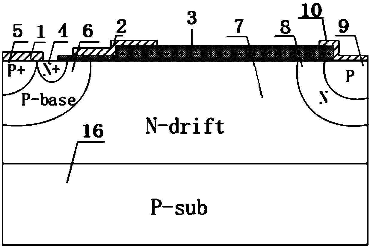
[0095] This embodiment provides a MOS control anode IGBT device, the cell structure of which is as follows figure 2 As shown, it includes an anode structure, a drift region structure, a cathode structure and a control gate structure located above the P+ substrate 116; wherein, the drift region structure is located on the upper surface of the P+ substrate 116, and the drift region structure includes an N-type drift region 107; The anode structure is located on one side of the top layer of the N-type drift region 107, and the anode structure includes an N-type buffer layer 108, a P-type anode region 109 located on the top layer of the N-type buffer layer 108, and an anode metal drawn from the P-type anode region 109 118; the cathode structure is located on the other side of the top layer of the N-type drift region 107, and the cathode structure includes a P-type body region 106, a P+ emitter region 105, an N+ emitter region 104 and a cathode metal 101; the P-type body region 106...

Embodiment 2

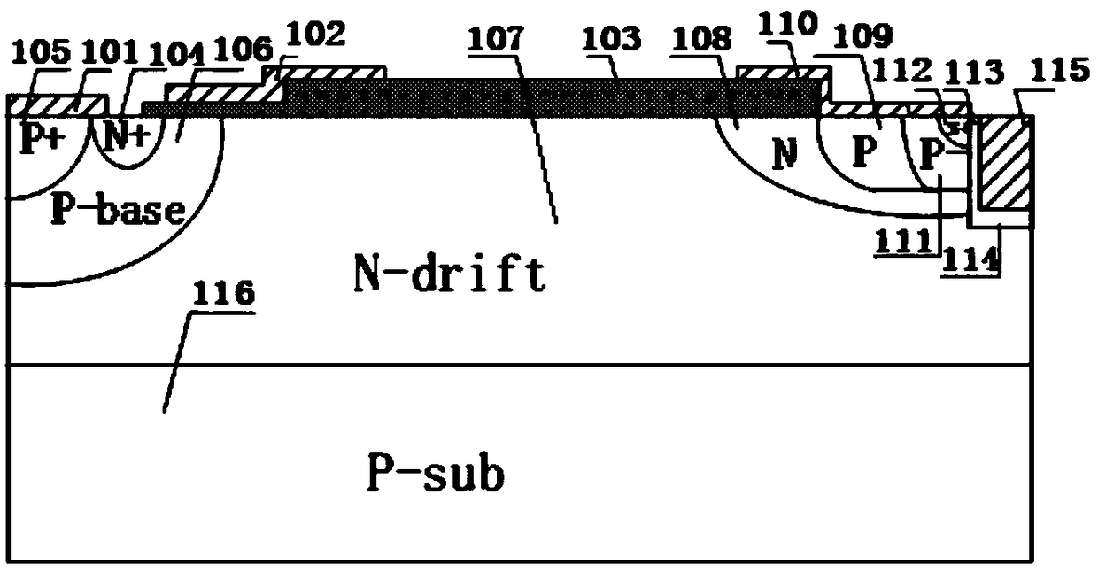
[0098] This embodiment provides a MOS control anode IGBT device, the cell structure of which is as follows image 3 As shown, the difference from Embodiment 1 is that the thickness of the second anode trench gate dielectric layer 114 in the anode trench gate structure is greater than the thickness of the first anode trench gate dielectric layer 113, specifically, the first anode trench gate The thickness of dielectric layer 113 is about The thickness of the second anode trench gate dielectric layer 114 is about The purpose of this design is to reduce the parasitic capacitance of the anode trench gate electrode while controlling the turn-on voltage of the anode trench gate, thereby reducing the adverse effect of the parasitic parameters of the anode MOS structure on the IGBT device parameters.

Embodiment 3

[0100] This embodiment provides a MOS control anode IGBT device, the cell structure of which is as follows Figure 4 As shown, the difference from Embodiment 1 is that the N+ source region 112 in the anode MOS structure is replaced with a P- base region 111 . Since the concentration of the P-base region 111 is lower than that of the P-type anode region 109, when the device is working, the anode trench gate controls the channel inversion on the side, thereby achieving the effect of bypassing the anode diode. At this time, the P-type anode region 109 forms an ohmic contact with the anode metal 110 , and the P-base region 111 forms a Schottky contact with the anode metal 110 .

[0101] When the device is working, the Schottky junction formed by the anode metal 110 and the P-base region 111 is reversely biased. When the control gate structure forms a conductive channel, the carriers passing through the channel of the control gate structure are reversely Under the action of the pa...


PUM


Abstract

A lateral bipolar semiconductor power device and a preparation method thereof belong to the technical field of semiconductor power device. When the cathode structure of the conventional bipolar powersemiconductor device is kept unchanged, by introducing an anode trench gate structure and a source region and / or a base region into the anode region of the device, the forward conduction voltage dropof the anode diode is bypassed by controlling the anode trench gate structure without affecting the normal operation and opening of the device, so that the effect of reducing the forward conduction voltage drop of the power semiconductor device is achieved. After the anode diode is bypassed, the minority carrier injection from the anode region to the drift region decreases, and the reverse recovery time of the device is shortened when the device is turned off, which improves the turn-off speed of the device and reduces the switching loss. The invention improves the carrier concentration distribution of the whole N-type drift region and the compromise between the positive conduction voltage drop and the switching loss. Moreover, the fabrication method of the device does not require additional process steps, and is compatible with the traditional device fabrication method.

Description

technical field [0001] The invention belongs to the technical field of power semiconductor devices and their preparation, and in particular relates to a bipolar semiconductor power device with a lateral MOS control anode and a preparation method thereof. Background technique [0002] As a major category of electronic technology, power electronics technology (another category is information electronics technology) is a technology that can realize the transmission, processing, storage and control of electric energy, and is suitable for high-power power conversion and processing. This technology can change the voltage, current, frequency, and phase to meet the power requirements of the system, so as to ensure the proper application of electric energy. In addition, electric energy can be used after being processed by power electronic technology, which can be more economical, efficient and environmentally friendly. Power electronics technology was born in the 1950s. As a new tec...

Claims


Application Information

Patent Timeline
Patent Type & Authority Applications(China)
IPC IPC(8): H01L29/06H01L21/336H01L29/739
CPCH01L29/0684H01L29/66325H01L29/7393
Inventor 张金平殷鹏飞赵阳刘竞秀李泽宏张波
Owner UNIV OF ELECTRONICS SCI & TECH OF CHINA
Why Eureka
Try Eureka