
Output/input circuit with small area

An I/O, circuit technology, applied in logic circuits, electrical components, pulse technology, etc., can solve problems such as the inability to reduce the area, and achieve the effect of reducing the total area, increasing the speed, and reducing the equivalent capacitance

Inactive Publication Date: 2009-08-19
FARADAY TECH CORP
View PDF0 Cites 8 Cited by
  • Summary
  • Abstract
  • Description
  • Claims
  • Application Information

AI Technical Summary

Problems solved by technology

[0006] Therefore, in order to overcome the shortcomings of the known technology that the external drive circuit needs to cooperate with the electrostatic discharge design rules and cannot reduce the area, the present invention provides a small-area input and output circuit, which uses an electrostatic discharge protection circuit for electrostatic discharge protection, and cooperates with resistors to form The electrostatic discharge blocking circuit is used to substantially prevent the electrostatic discharge current from entering the external drive circuit, so as to release (relax) the design rule restrictions of the external drive circuit (for example, the electrostatic discharge design rule), so that each external drive circuit At least one transistor can be implemented in a single finger layout, which can not only reduce the equivalent capacitance of the external drive circuit, increase its speed, reduce switching power consumption, but also effectively reduce the output and output circuits the overall area of

Method used


Image

  • Output/input circuit with small area
  • Output/input circuit with small area
  • Output/input circuit with small area

Examples


Embodiment Construction

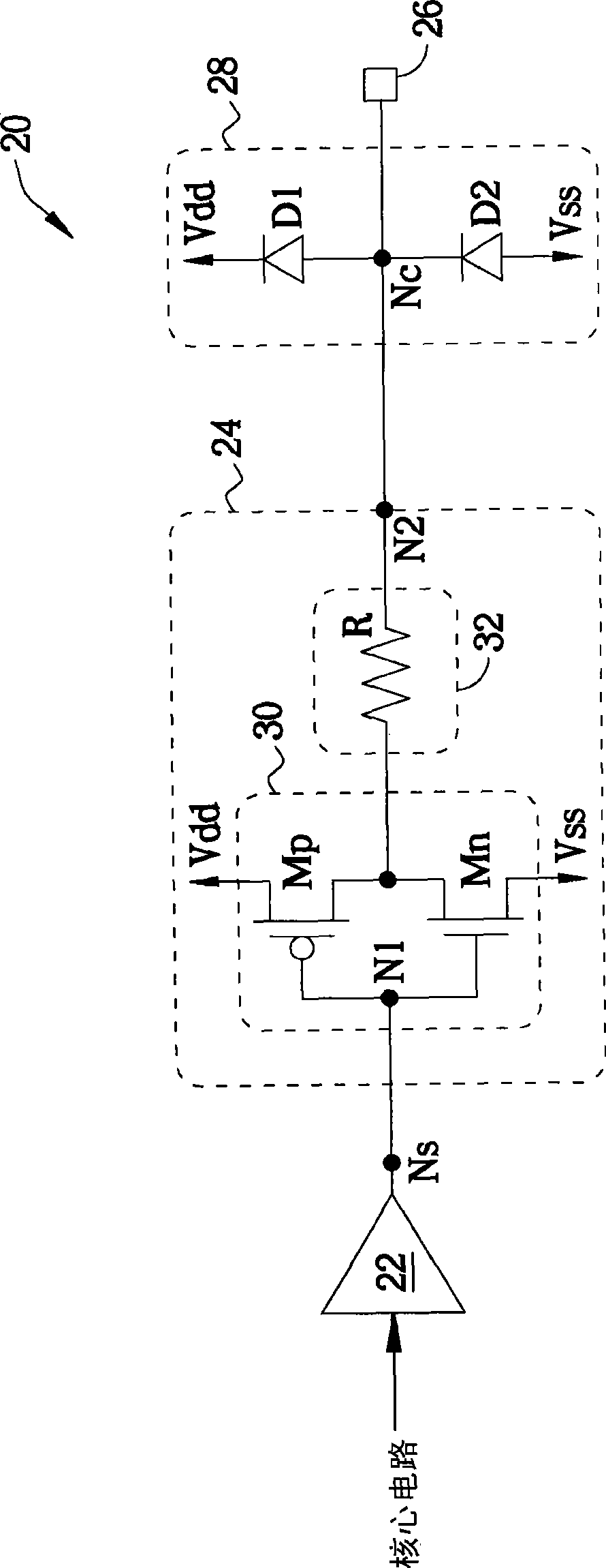
[0043] Please refer to figure 2 ; figure 2 It is a schematic circuit diagram of the first embodiment 20 of the input-output circuit of the present invention. The I / O circuit 20 operates between voltage levels Vdd and Vss, and is provided with an I / O pad 26 (pad), an ESD protection circuit 28 and a circuit unit 24 . Wherein, the I / O circuit 20 is set in a chip to drive other circuits outside the chip, and the I / O pad 26 is used to connect other circuits outside the chip. The electrostatic discharge protection circuit 28 is connected to the I / O pad 26, and the node Nc can be regarded as a connection end; the pre-driver 22 of the matching circuit unit 24 forms a signal end at the node Ns. On the other hand, the nodes N1 and N2 of the circuit unit 24 can be regarded as a first end and a second end, respectively connected to a signal end (node ​​Ns) and a connection end (node ​​Nc). The circuit unit 24 is also provided with a driving circuit 30 (that is, an off-chip driving ci...


PUM


Abstract

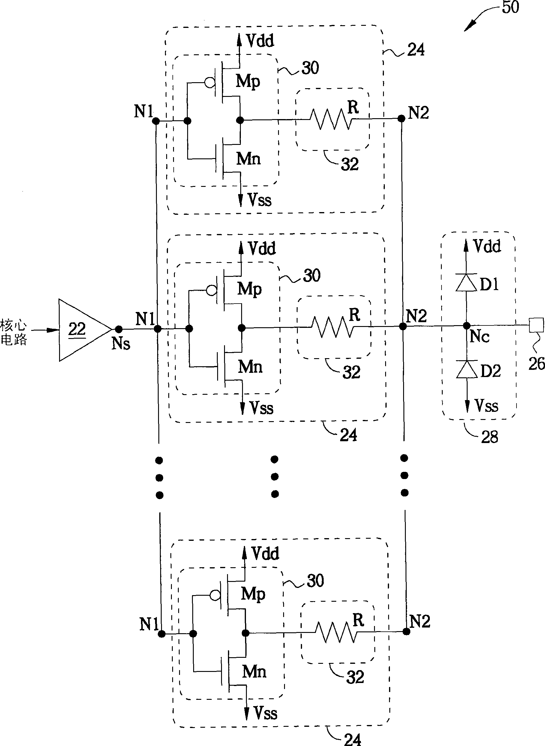
The invention provides an input and output circuit with small area, wherein, one or a plurality of parallelly connected circuit units and a static discharge protection circuit are arranged between a core circuit / a pre-driver and an input and output pad. An ex-core drive circuit and a resistance of an output end are arranged in each circuit unit, wherein, the static discharge protection circuit can avoid static discharge incidents on the input and output pad, and the resistance in each circuit unit realizes the static discharge barrier function so as to prevent static discharge current from entering corresponding drive circuits, thus leading transistors in the drive circuits not to be subjected to design rules of static discharge and realizing single finger layout to reduce the equivalent capacitance of the drive circuits. Therefore, the total areas of the drive circuits and the whole input and output circuit can be effectively reduced so as to realize the input and output circuit with small area.

Description

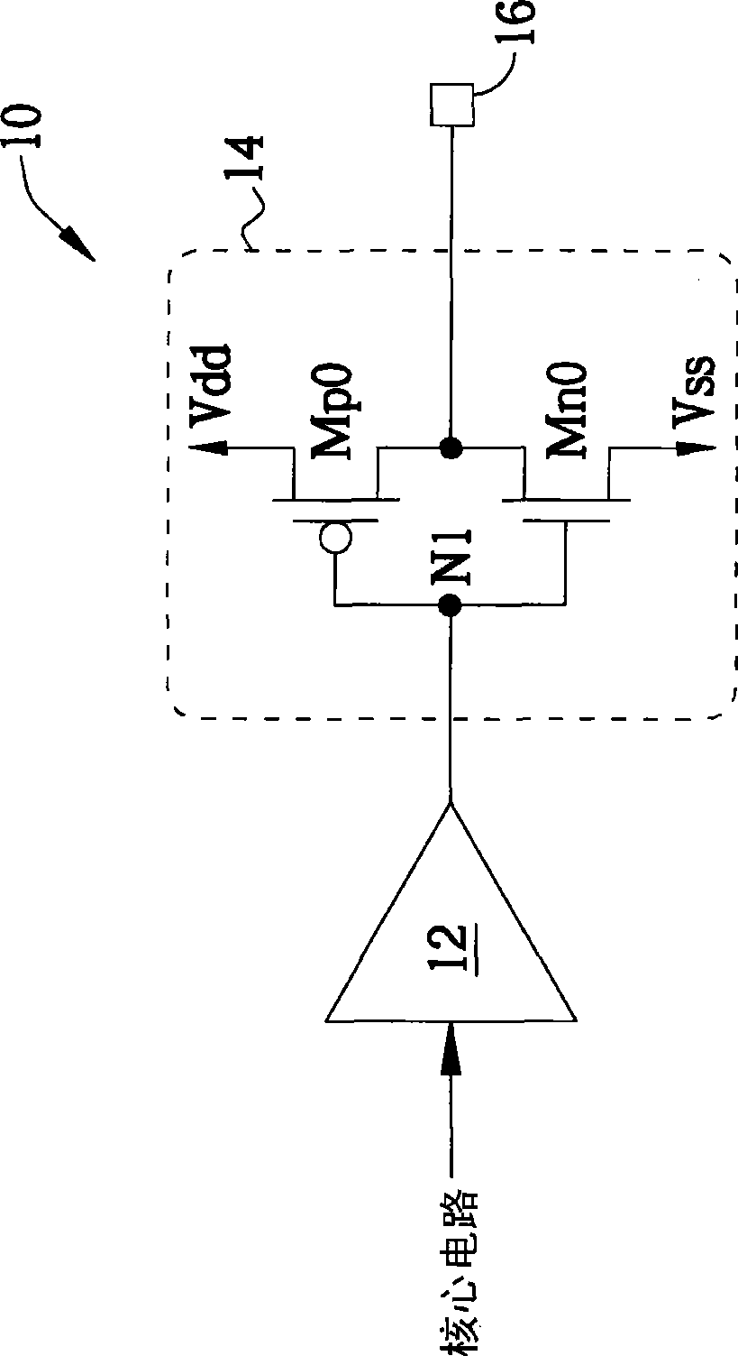
technical field [0001] The present invention relates to a small-area I / O circuit, in particular to an I / O circuit that can use resistance to block electrostatic discharge paths to reduce the area of ​​an off-chip driver and the overall area of ​​the I / O circuit. Background technique [0002] Chips are the most important hardware foundation of the modern information society. In order to make the use of chips more popular, improving the integration of chips and reducing the size of chips has become the focus of modern chip design, manufacturing and research and development. [0003] As known to those skilled in the art, the chip is provided with input and output circuits so that the chip can exchange signals with other circuits outside the chip. Please refer to figure 1 . figure 1 That is, it is a schematic circuit diagram of an I / O circuit 10 in the prior art. Cooperating with a pre-driver 12 , an off-chip driver 14 is provided in the I / O circuit 10 . The signal output b...

Claims


Application Information

Patent Timeline
IPC IPC(8): H03K19/00
Inventor 吴志宏张鸿仪洪国钟
Owner FARADAY TECH CORP
Learn More