Light trapping structure for thin film solar cell

A technology of thin-film solar cells and light-trapping structures, applied in the field of light-trapping structures, can solve the problems of inconspicuousness, complicated preparation process, and high cost of solar cells, and achieve the effects of easy processing and production, large light-trapping efficiency, and high light-trapping efficiency

Inactive Publication Date: 2011-01-26
INST OF ELECTRICAL ENG CHINESE ACAD OF SCI
View PDF5 Cites 1 Cited by
  • Summary
  • Abstract
  • Description
  • Claims
  • Application Information

AI Technical Summary

Problems solved by technology

However, as an integral part of the overall energy structure of society, the proportion of solar energy is still less than 1% at present. The main reason for this situation is that the cost of solar cells is too high
Some of these structures do not increase the light trapping effect significantly, and some have complex preparation processes

Method used


Image

  • Light trapping structure for thin film solar cell
  • Light trapping structure for thin film solar cell
  • Light trapping structure for thin film solar cell

Examples


Embodiment 1

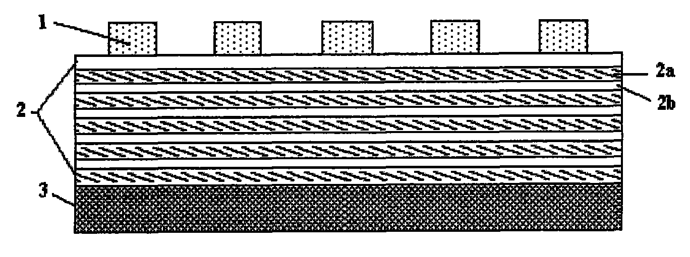
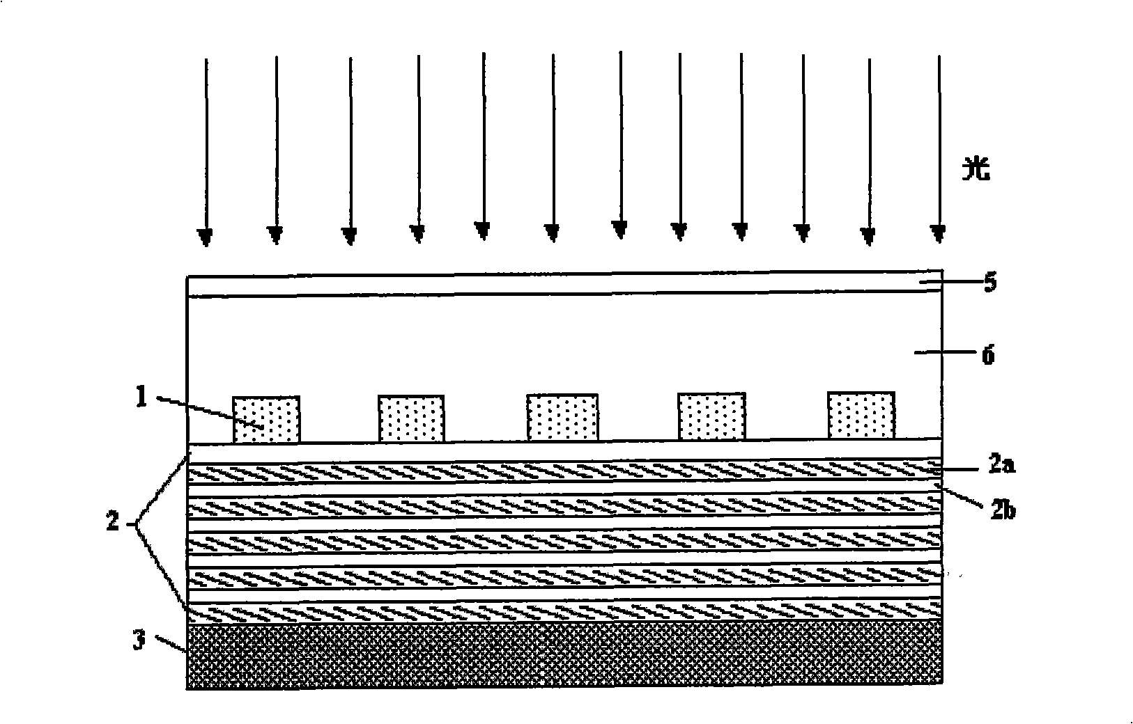
[0027] Such as image 3 As shown in , a light-trapping structure of the present invention is applied to the backlight surface of a thin-film silicon solar cell. In the figure, 1 is a diffraction grating, 2 is a distributed Bragg reflector (DBR), 2a and 2b are two material layers with different refractive indices that constitute the DBR, 3 is a metal reflector, 5 is an ITO anti-reflection coating, 6 It is a thin film silicon layer; wherein, the diffraction grating 1, the distributed Bragg reflector (DBR) 2 and the metal reflector 3 jointly constitute a light trapping structure of the present invention. In this embodiment, the constituent material of the diffraction grating 1 is indium tin oxide (ITO), the constituent material of the distributed Bragg reflector (DBR) 2 is 2a: doped a-Si, 2b: ITO, and the composition of the metal reflector 3 The material is Ag. The light-trapping structure of the present invention thus obtained is conductive.

[0028] When the thickness of the...

Embodiment 2

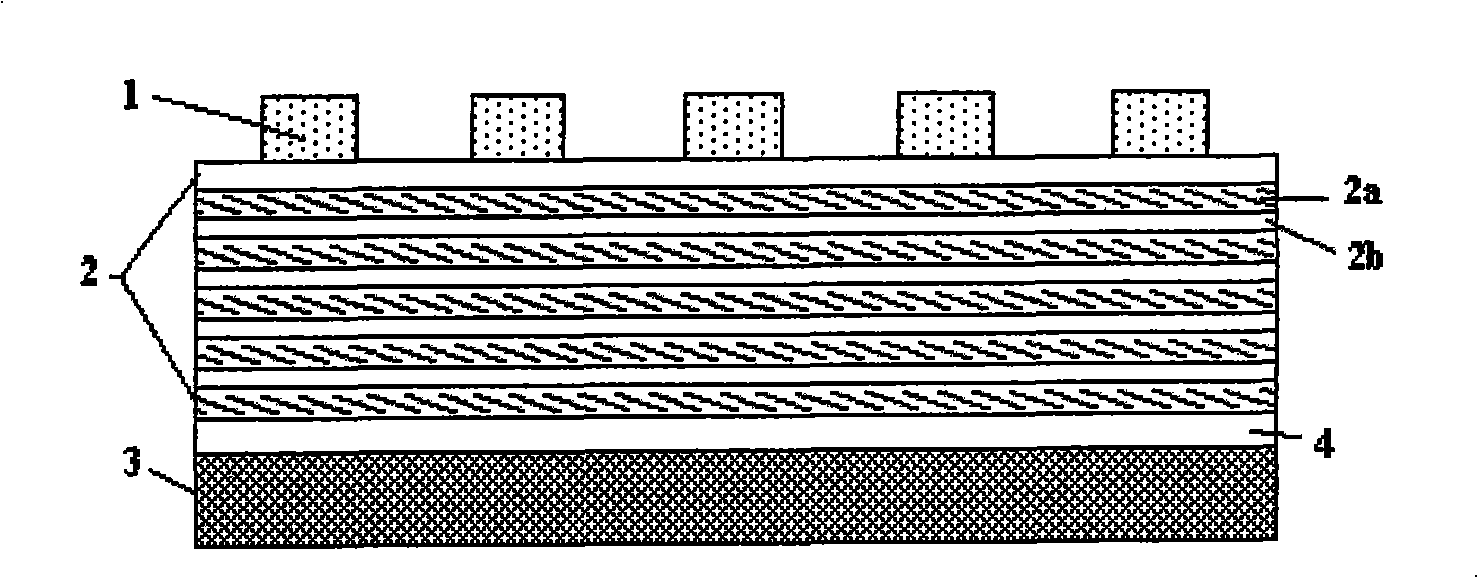
[0030] Such as Figure 5 As shown in , a light-trapping structure of the present invention is applied to the backlight surface of a thin-film silicon solar cell. In the figure, 1 is a diffraction grating, 2 is a distributed Bragg reflector (DBR), 2a and 2b are two material layers with different refractive indices that constitute the DBR, 3 is a metal reflector, 4 is a dielectric buffer layer, and 5 is ITO The anti-reflection coating, 6, is a thin film silicon layer; wherein, the diffraction grating 1, the distributed Bragg reflector (DBR) 2, the metal reflector 3 and the dielectric buffer layer 4 together constitute a light trapping structure of the present invention. In this embodiment, the constituent material of the diffraction grating 1 is indium tin oxide (ITO), the constituent material of the distributed Bragg reflector (DBR) 2 is 2a: doped a-Si, 2b: ITO, and the composition of the metal reflector 3 The material is Ag, and the constituent material of the dielectric buff...


PUM


Abstract

The invention relates to a light trapping structure for a thin film solar cell, which is basically characterized by being positioned at the back light surface of a solar cell light absorbing area, a dThe invention relates to a light trapping structure for a thin film solar cell, which is basically characterized by being positioned at the back light surface of a solar cell light absorbing area, a diffraction grating 1, a distributed Bragg reflector (DBR) 2 and a metal reflector 3 are sequentially arranged from one side of the solar cell light absorbing area, wherein the diffraction grating 1 iniffraction grating 1, a distributed Bragg reflector (DBR) 2 and a metal reflector 3 are sequentially arranged from one side of the solar cell light absorbing area, wherein the diffraction grating 1 increases light diffraction efficiency, the DBR2 and the metal reflector 3 jointly increase the reflectivity of the light, and the metal reflector 3 can greatly increase the light trapping efficiency ofcreases light diffraction efficiency, the DBR2 and the metal reflector 3 jointly increase the reflectivity of the light, and the metal reflector 3 can greatly increase the light trapping efficiency ofthe light trapping structure and reduce the pair numbers of the DBR 2, so that the light trapping structure can be easily manufactured; and a medium buffering layer 4 can be further arranged between the light trapping structure and reduce the pair numbers of the DBR 2, so that the light trapping structure can be easily manufactured; and a medium buffering layer 4 can be further arranged betweenthe DBR 2 and the metal reflector 3.the DBR 2 and the metal reflector 3.

Description

technical field [0001] The invention relates to the field of solar cells, in particular to a light-trapping structure for thin-film solar cells. Background technique [0002] The development and utilization of solar energy has become a strategic decision for sustainable energy development in countries all over the world. Both developed countries and developing countries have formulated medium and long-term development plans, taking photovoltaic power generation as the hope of human future energy. However, as an integral part of the overall energy structure of society, the proportion of solar energy is still less than 1% at present. The main reason for this situation is that the cost of solar cells is too high. At present, the retail price of crystalline silicon solar cell modules, which accounts for nearly 90% of the photovoltaic market, is still at 4.78$ / Wp, and the most important cost is the cost of silicon wafers with a thickness of about 170-220 microns. [0003] There...

Claims


Application Information

Patent Timeline
Patent Type & Authority Patents(China)
IPC IPC(8): H01L31/0232H01L31/054
CPCY02E10/52
Inventor 赵雷王文静
Owner INST OF ELECTRICAL ENG CHINESE ACAD OF SCI
Why Eureka
Try Eureka