Check patentability & draft patents in minutes with Patsnap Eureka AI!

Multilink microstrip conducting wire and design method thereof

A technology of multiple connections and design methods, applied in the direction of connection devices, waveguides, antennas, etc., can solve problems such as interference

Inactive Publication Date: 2009-09-09
倪其良
View PDF2 Cites 0 Cited by
  • Summary
  • Abstract
  • Description
  • Claims
  • Application Information

AI Technical Summary

Problems solved by technology

But it is also susceptible to interference from external signals and adjacent electromagnetic structures

Method used


Image

  • Multilink microstrip conducting wire and design method thereof
  • Multilink microstrip conducting wire and design method thereof
  • Multilink microstrip conducting wire and design method thereof

Examples


Embodiment Construction

[0027] Below in conjunction with accompanying drawing, above-mentioned and other technical characteristics and advantages of the present invention are described in detail:

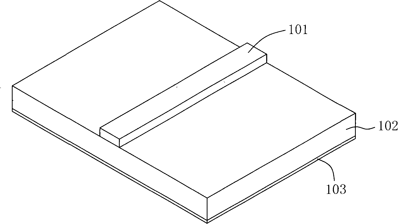
[0028] figure 1 It is an existing traditional microstrip wire, including a signal conductor 101 , a dielectric 102 , and a ground conductor 103 .

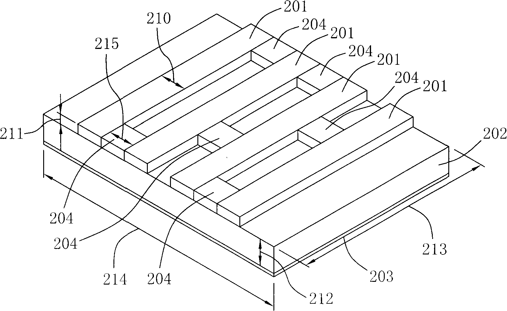
[0029] figure 2 It is the multi-connection microstrip wire of the present invention, including: signal conductor 201, dielectric substance 202, ground conductor 203, conductor segment 204 connecting signal conductor 201, and the width 210 and height 211 of signal conductor 201, the height of dielectric substance 212 and length 213. The width 214 of the limited area ground conductor. Multiconnection microstrip conductors have two or more signal conductors. The distance 215 between the signal conductors is the width of the conductor segment connecting the signal conductors. The distance and width between individual signal conductors 201 do not have to be th...


PUM


Abstract

The invention relates to a multilink microstrip conducting wire and a design method thereof. A plurality of groups of microstrip conducting wires are used as conductor sections which are connected into an electrically conducted multilink microstrip conducting wire structure. The multilink microstrip conducting wire improves the characteristics of a plurality of conventional microstrip conducting wires, and avoids the defect that the conventional microstrip conducting wires are easily interfered by external signals and adjacent electromagnetic structures. The design method uses the multilink microstrip lead which brings about easier wideband matching than the conventional microstrip conducting wire, reduces the interference and improves the Q value. The design method designs a component having the functions of conduction, feed-in / feed-out, storage / release, and transmission / reception. The method aims at providing the design and manufacture of a component which has the functions of conduction, feed-in / feed-out, and transmission / reception and is applied to metal and semimetal and dielectric materials such as antennae, conducting wires, components with the function of electromagnetic energy storage / release such as inductance, and single-layer or multilayer dielectrics such as integrated circuits, thin film transistor circuits, low temperature or high temperature co-burnt ceramics, printed circuit boards, PC soft plates, nanometer carbon tubes, and the like.

Description

technical field [0001] The present invention relates to a microstrip wire structure and design method thereof, especially to a multiple-connected microstrip wire (multiple-connected micro strip line) structure, so that it can improve the characteristics of many traditional microstrip wires, but still maintain the simple structure of traditional microstrip wires to improve its use efficiency and application range. Background technique [0002] Microstrip lines have broadband characteristics, and have been widely used as telecommunication conduction, feed-in / out-feed, storage / release, and transmit / receive structures for many years, and the examples are too numerous to enumerate. The main advantage is that its structure is simple, so it is easy to manufacture and connect and integrate with other structures. But it is also susceptible to interference from external signals and adjacent electromagnetic structures. The reference papers are as follows: [0003] H.A. Wheeler, "Tra...

Claims


Application Information

Patent Timeline
Patent Type & Authority Applications(China)
IPC IPC(8): H01P5/10H01P3/08H01Q13/08
Inventor 倪其良
Owner 倪其良
Features
  • R&D
  • Intellectual Property
  • Life Sciences
  • Materials
  • Tech Scout
  • Unparalleled Data Quality
  • Higher Quality Content
  • 60% Fewer Hallucinations
Learn More