Inverse integrator of lower-gain switch capacitance with non-sensitive parasitic effect and lower power consumption
A parasitic effect, gain switching technology, applied in differential amplifiers, DC-coupled DC amplifiers, electrical components, etc., can solve problems such as sensitivity to capacitance parasitics
- Summary
- Abstract
- Description
- Claims
- Application Information
AI Technical Summary
Problems solved by technology
Method used
Image

Examples
Embodiment Construction
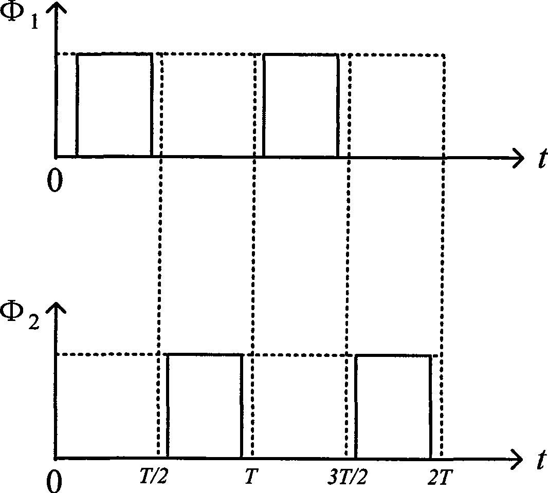
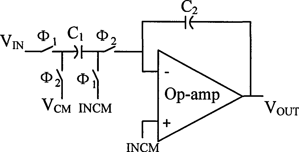
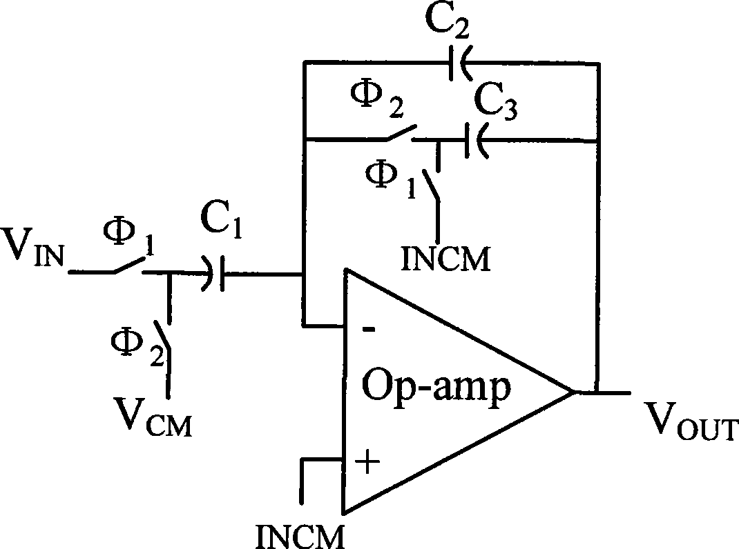
[0037] The working process of the small-gain switched capacitor inverting integrator with insensitive parasitic effect and low power consumption of the present invention is as follows:
[0038] 1. At sampling phase φ 1 When , the first switch, the fourth switch and the sixth switch are turned on, and the input voltage V IN Sampled capacitance C 1 , the third capacitor C 3 and the fourth capacitor C 4 Composed of capacitive network sampling. At sampling phase φ 1 end, the sampling capacitor C 1 , the third capacitor C 3 and the fourth capacitor C 4 A certain charge is stored on them.
[0039] 2. In the integral phase φ 2 When , the second switch, the third switch, the fifth switch and the seventh switch are turned on, and the sampling capacitor C 1 The two ends are short-circuited, and the charge on it is cleared. Fourth capacitor C 4 Both ends are connected to a common-mode voltage, and the charge on it is also zeroed. The third capacitor C 3 The charge on the op...
PUM
 Abstract
Description
Claims
Application Information
 - R&D
- Intellectual Property
- Life Sciences
- Materials
- Tech Scout
- Unparalleled Data Quality
- Higher Quality Content
- 60% Fewer Hallucinations
Browse by: Latest US Patents, China's latest patents, Technical Efficacy Thesaurus, Application Domain, Technology Topic, Popular Technical Reports.
© 2025 PatSnap. All rights reserved.Legal|Privacy policy|Modern Slavery Act Transparency Statement|Sitemap|About US| Contact US: help@patsnap.com