Method of manufacturing semiconductor chip

一种制造方法、半导体的技术,应用在半导体/固态器件制造、半导体器件、电固体器件等方向,能够解决测试图案除去等问题,达到通用特性保证、高效率的效果

Active Publication Date: 2009-09-23
PANASONIC CORP
View PDF4 Cites 49 Cited by
  • Summary
  • Abstract
  • Description
  • Claims
  • Application Information

AI Technical Summary

Problems solved by technology

That is, when the general characteristics are guaranteed, the test pattern cannot be efficiently removed by simple steps in the division step

Method used


Image

  • Method of manufacturing semiconductor chip
  • Method of manufacturing semiconductor chip
  • Method of manufacturing semiconductor chip

Examples


Embodiment Construction

[0029] Embodiment modes of the present invention are described below with reference to the drawings.

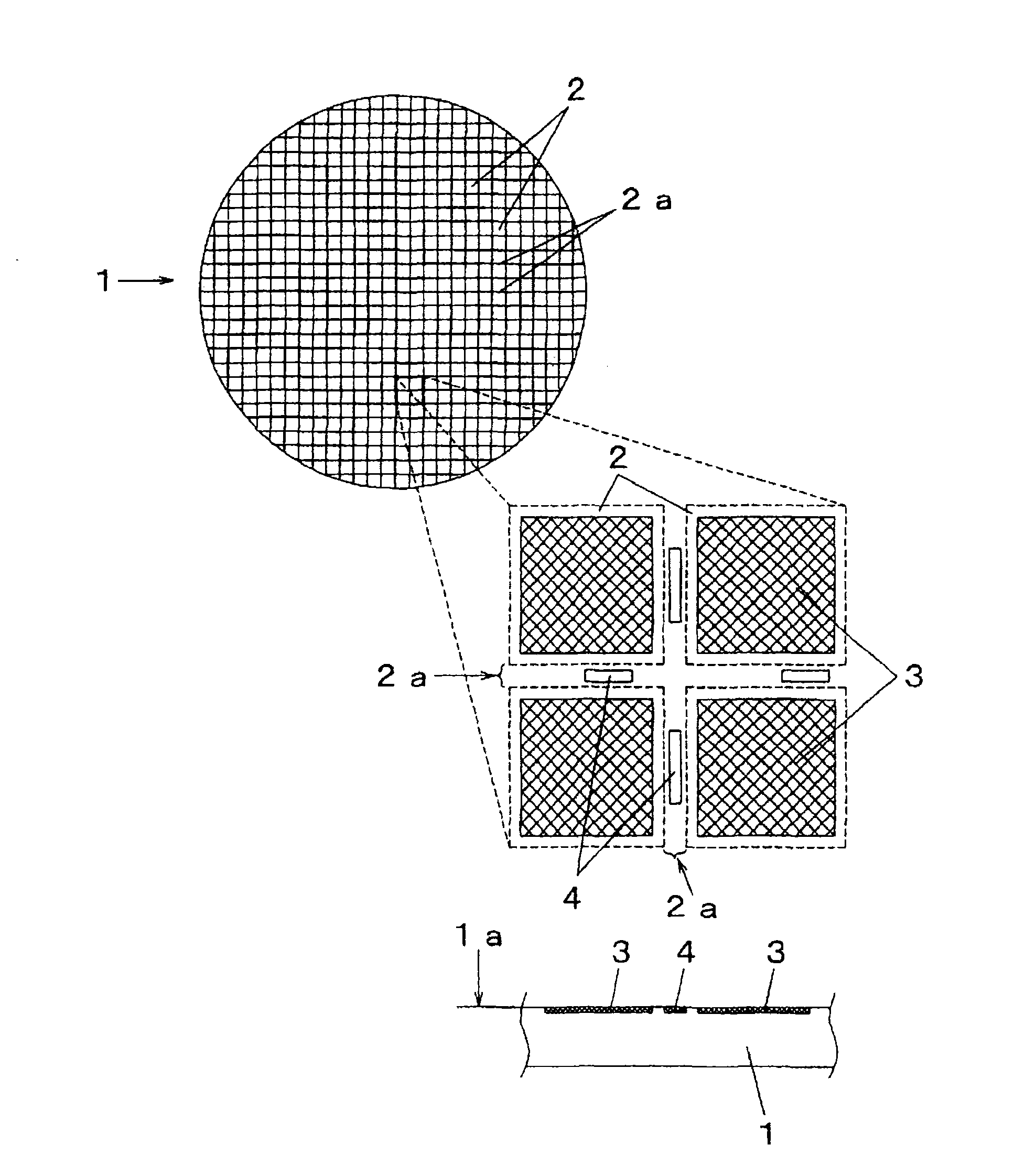
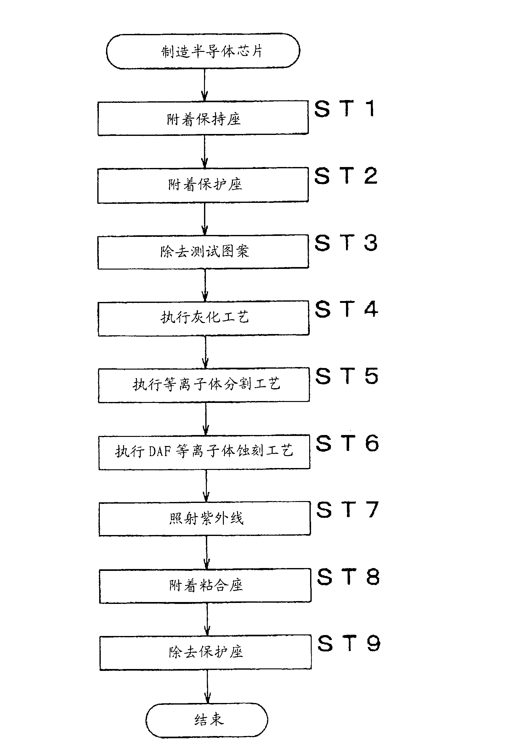
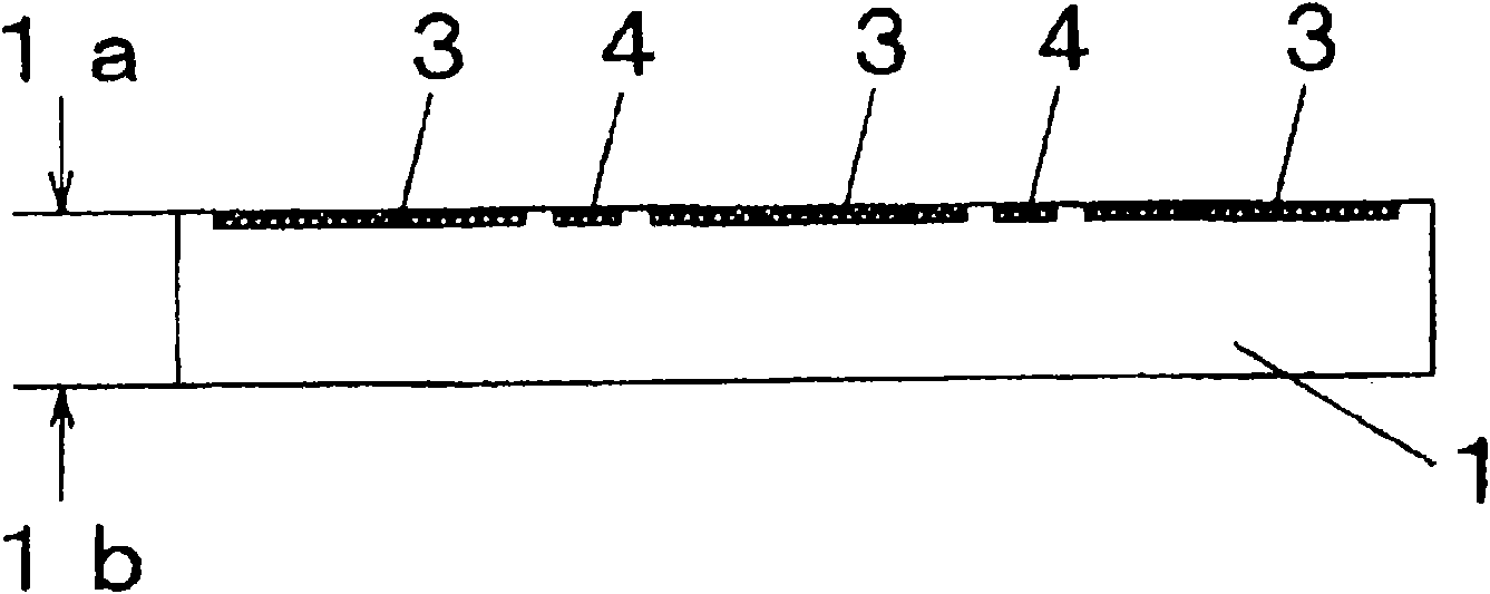
[0030] First, refer to figure 1 The semiconductor wafer 1 used in the semiconductor chip manufacturing method of the embodiment mode of the present invention will be described. exist figure 1 In , the semiconductor wafer 1 has been partitioned into a plurality of chip regions 2 (regions) in a rectangular shape by using scribe lines 2a arranged in a lattice shape, thereby cutting the respective semiconductor chips from each other. On the front side 1a opposite to the circuit formation side of the semiconductor wafer 1, each integrated circuit 3 has been formed in each chip region 2, and test patterns 4 have been formed in the scribe lines 2a. The test pattern 4 is used for characteristic tests and the like in the semiconductor chip manufacturing steps, and is removed after the function of the test pattern 4 has been achieved. In the semiconductor chip manufacturing method s...


PUM


Abstract

In a method in which a semiconductor wafer 1 having integrated circuits 3 formed in a plurality of chip regions and test patterns 4 formed in scribe lines 2a is divided by a plasma etching process so as to manufacture individual semiconductor chips, in the semiconductor wafer 1, a protection seat 5 which constitutes a mask in the plasma etching process is adhered onto a front plane 1a thereof where the integrated circuits 3 have been formed; since laser light 9a is irradiated along the scribe lines 2a, only a predetermined width of the protection seat 5 is removed so as to form a mask having a plasma dicing-purpose opening portion 5b; and also, the test patterns 4 are removed by the laser light 9a in combination with a front plane layer of the semiconductor wafer 1. As a result, the test patterns 4 can be removed in a higher efficiency and in simple steps, while the general purpose characteristic can be secured.

Description

technical field [0001] The present invention relates to a semiconductor chip manufacturing method for manufacturing semiconductor chips by dividing a semiconductor wafer on which test patterns have been formed on scribe lines with respect to each integrated circuit. Background technique [0002] Semiconductor chips are manufactured in such a manner that after a plurality of integrated circuits have been formed in batch mode in the case of a semiconductor wafer, the semiconductor wafer is diced along scribe lines to be divided with respect to each integrated circuit. Although various wafer dicing methods have been conventionally employed, for example, a wafer dicing method is known in which the wafer is mechanically diced using a rotary blade (for example, see Patent Document 1); A wafer dicing method is known, such as a method based on a plasma dividing process in which a portion of the wafer corresponding to a scribe line is removed by a plasma etching process to divide the...

Claims


Application Information

Patent Timeline
Patent Type & Authority Applications(China)
IPC IPC(8): H01L21/78
CPCH01L21/78H01L21/6836H01L2221/68327H01L2221/68377H01L2221/68381
Inventor 有田洁针贝笃史
Owner PANASONIC CORP
Why Eureka
Try Eureka