Check patentability & draft patents in minutes with Patsnap Eureka AI!

Method for assembling microwire electrode array by using silicon array hole

A technology of microwire electrodes and array holes, which is applied in the field of assembly of microwire electrode arrays, can solve the problems of poor device consistency, difficult position fixation, and low yield.

Inactive Publication Date: 2010-09-15
INST OF SEMICONDUCTORS - CHINESE ACAD OF SCI
View PDF0 Cites 0 Cited by
  • Summary
  • Abstract
  • Description
  • Claims
  • Application Information

AI Technical Summary

Problems solved by technology

The diameter of the microwire electrode used for neural signal recording is generally less than 100 μm, which is easy to bend and not easy to fix the position during the production process, which makes the yield of the product low and the consistency of the device is not good

Method used


Image

  • Method for assembling microwire electrode array by using silicon array hole
  • Method for assembling microwire electrode array by using silicon array hole
  • Method for assembling microwire electrode array by using silicon array hole

Examples


Embodiment Construction

[0026] In order to make the object, technical solution and advantages of the present invention clearer, the present invention will be described in further detail below in conjunction with specific embodiments and with reference to the accompanying drawings.

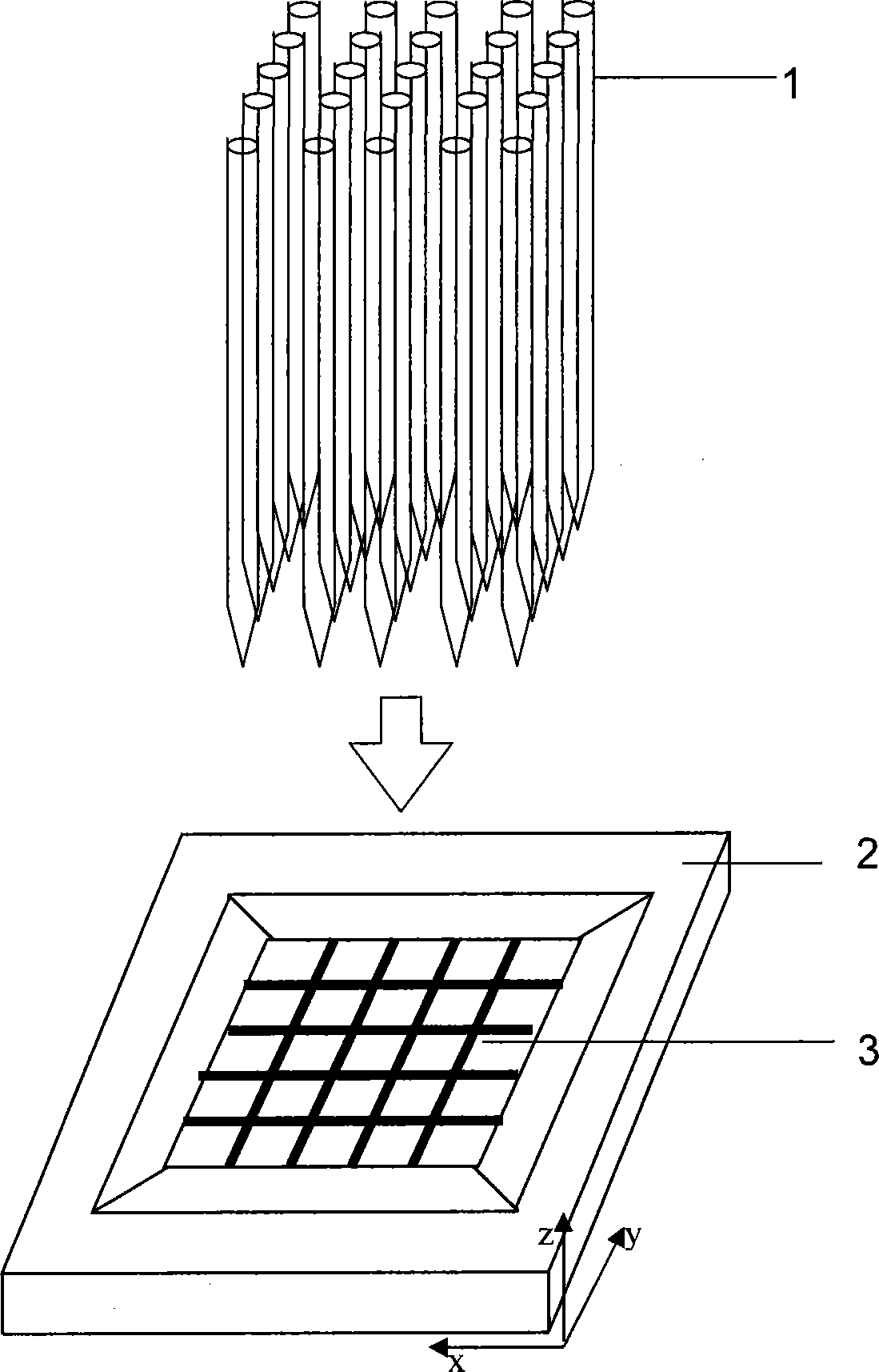
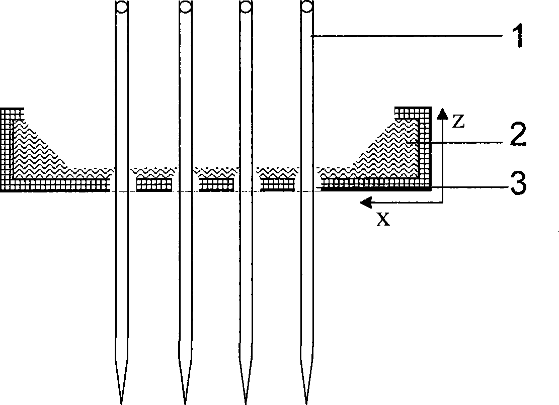
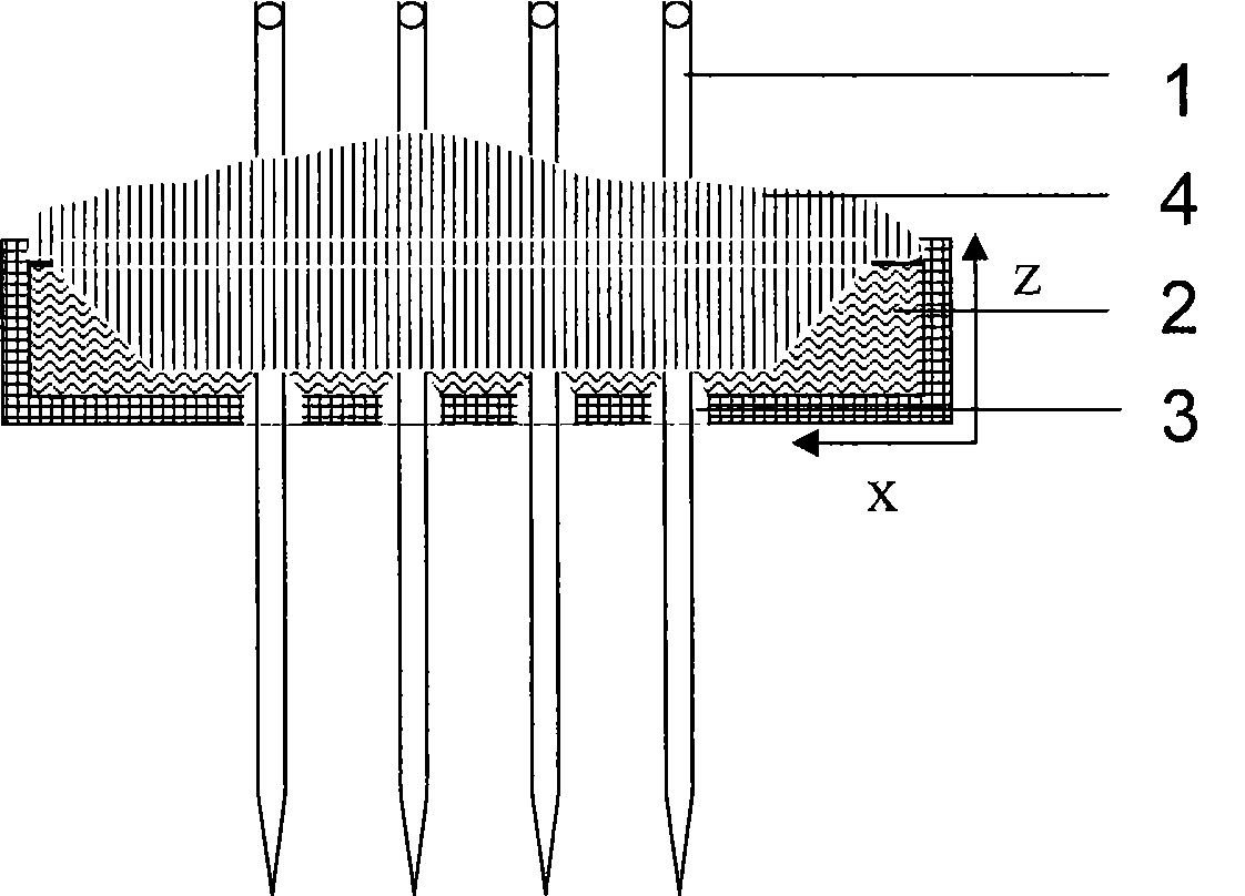
[0027] 1. Determine the hole size of the silicon array. Determine the size of the hole according to the diameter of the microfilament, which should be slightly larger than the diameter of the microfilament. Silicon single crystal has the property of anisotropy, using this property to use the silicon wafer with the surface of (100) crystal plane, through the method of chemical anisotropic etching, the array holes with high precision and smooth side wall can be fabricated. Since the angle between the (110) plane and the (111) plane of the silicon wafer is 54.7°, the opening size of the array holes and the thickness of the frame determine the size of the holes after etching. The relationship between the hole opening size L,...


PUM

PropertyMeasurementUnit
diameteraaaaaaaaaa

Abstract

The invention relates to an assembling technology of a microwire electrode array, in particular to a technology of assembling a microwire electrode by using a silicon array hole. By adopting a common photoetching and chemical anisotropic etching method, the silicon array hole with high precision, low cost and controllable aperture and layout way can be manufactured, and the two-dimensional or thethree-dimensional assembling of the microwire electrode is finished through the fixation of epoxy resin. The method is suitable for the assembly of the small-size microwire electrode array and the device encapsulation, and the array hole can be customized according to the radius, spacing and layout way, and the like of the microwire.

Description

technical field [0001] The invention relates to the assembly technology of microwire electrode arrays, in particular to a technology for assembling microwire electrodes using silicon array holes. Background technique [0002] When a person is thinking, there will be specific electrical activity in the cerebral cortex, which is called EEG. The study of EEG signals is an important means to understand the mechanism of human brain activity, human cognitive process and diagnosis of brain diseases, and it is also a new way to realize the communication between human and the outside world. [0003] In order to gain a deep understanding of the mechanism of brain activity and the interaction between neurons, we need effective tools to record EEG signals. Advances in MEMS technology and micro-nano processing technology have prompted us to manufacture a variety of new neural signal recording electrodes, such as microwire electrodes, planar electrodes, and three-dimensional electrodes. ...

Claims


Application Information

Patent Timeline
Patent Type & Authority Patents(China)
IPC IPC(8): A61B5/0478B81C1/00
Inventor 陈弘达朱琳裴为华张旭
Owner INST OF SEMICONDUCTORS - CHINESE ACAD OF SCI
Features
  • R&D
  • Intellectual Property
  • Life Sciences
  • Materials
  • Tech Scout
  • Unparalleled Data Quality
  • Higher Quality Content
  • 60% Fewer Hallucinations
Learn More