Thin film transistor manufacturing method and display having the same

A thin-film transistor and display technology, which is applied in semiconductor/solid-state device manufacturing, electric solid-state devices, semiconductor devices, etc., can solve the problems of low yield rate of AMOLED products, uneven stripe-like light emission, etc.

Active Publication Date: 2009-09-30
INNOLUX CORP
View PDF3 Cites 9 Cited by
  • Summary
  • Abstract
  • Description
  • Claims
  • Application Information

AI Technical Summary

Problems solved by technology

[0004] When the display is made, factors such as standard laser technology and current drive related to driving thin film transistors will cause stripe-like uneven light emission (Stripe Mura), resulting in low yield of AMOLED products

Method used


Image

  • Thin film transistor manufacturing method and display having the same
  • Thin film transistor manufacturing method and display having the same
  • Thin film transistor manufacturing method and display having the same

Examples


Embodiment Construction

[0015] The technical content of the present invention will be described in detail below with reference to the drawings.

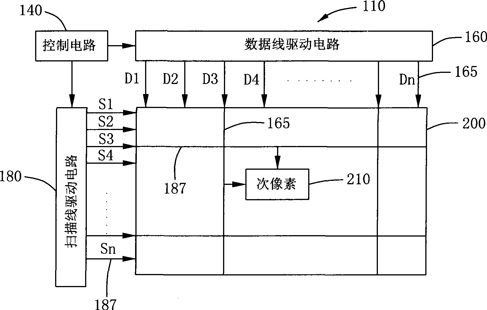
[0016] figure 1 The basic circuit structure of an active matrix organic light emitting diode (AMOLED) display 110 is shown. The OLED display 110 includes a control circuit 140 , a data line driving circuit 160 , a scanning line driving circuit 180 and a display panel 200 . The display panel 200 has a plurality of sub-pixels 210, and each pixel 210 is connected to a data line (D1 to Dn) 165 and a scan line (S1 to Sn) 187 to form a matrix. The sub-pixel 210 receives the image data signal of the data line driving circuit 160 and the switching / addressing signal of the scanning line driving circuit 180 via the data line 165 and the scanning line 187 . The data line driving circuit 160 and the scanning line driving circuit 180 are controlled by the control circuit 140 .

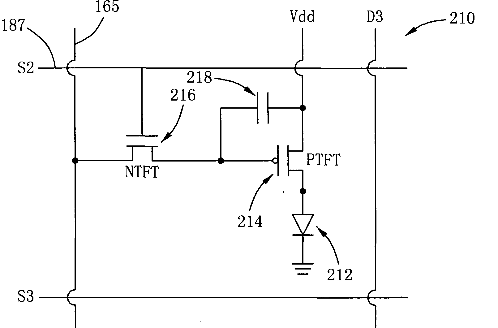
[0017] The circuit design of a sub-pixel may include a plurality of thin film transistors...


PUM


Abstract

An organic light emitting diode (OLED) display and thin film transistor (TFT) manufacturing method thereof are disclosed. According to the present invention, poly-silicon layers for forming active areas of non-driving TFT (e.g. peripheral circuit TFT and switch TFT) and driving TFT used in the OLED display are respectively made by using standard laser crystallization method and non-laser crystallization method or low energy laser crystallization method. Therefore, the peripheral circuit TFT has excellent electrical performance such as high carrier mobility, while the OLED-driving TFT has goodstability so that the resultant display can operate with improved luminance uniformity.

Description

technical field [0001] The present invention relates to an active matrix organic light emitting diode (Active Matrix Organic Light Emitting Diode; AMOLED) display, more specifically, relates to a method for manufacturing different thin film transistors (Thin Film Transistor; TFT) used in the AMOLED display, and includes the Active-matrix organic light-emitting diode displays such as thin-film transistors. Background technique [0002] Organic Light Emitting Diodes (OLEDs) have been widely used in displays, among which in Active Matrix Organic Light Emitting Diodes (AMOLED) displays, the light-emitting part uses a driving circuit to drive a light-emitting component—the Organic Light-Emitting Diode (OLED). The AMOLED driving circuit uses thin film transistors, including a switching thin film transistor (Switch Thin Film Transistor) and a driving thin film transistor (DrivingThin Film Transistor), wherein the switching thin film transistor is implemented as an N-type thin film ...

Claims


Application Information

Patent Timeline
Patent Type & Authority Applications(China)
IPC IPC(8): H01L21/84H01L27/32
CPCH01L27/1229H01L27/1251
Inventor 万德昌刘侑宗李淂裕
Owner INNOLUX CORP
Why Eureka
Try Eureka