SOI CMOS image sensor structure and manufacturing method thereof

A technology of image sensor and manufacturing method, which is applied in semiconductor/solid-state device manufacturing, radiation control devices, electrical components, etc., can solve the problems of increasing silicon film, reducing light absorption efficiency, limiting the thickness of photodiode depletion layer, etc., and achieving low Soft error probability, effect of low power consumption

Inactive Publication Date: 2009-09-30
BEIJING SUPERPIX MICRO TECHNOLOGY CO LTD
View PDF0 Cites 25 Cited by
  • Summary
  • Abstract
  • Description
  • Claims
  • Application Information

AI Technical Summary

Problems solved by technology

[0009] When using SOI to make a CMOS image sensor, because the thickness of the silicon film of SOI is thin, it is limited to make a photosensitive diode on it.
The thinner silicon film limits the thickness of the depletion layer of the photodiode, and the light absorption efficiency decreases
Increasing the thickness of the silicon film will not make fully depleted SOI devices, or reduce the radiation resistance of partially depleted SOI devices

Method used


Image

  • SOI CMOS image sensor structure and manufacturing method thereof
  • SOI CMOS image sensor structure and manufacturing method thereof
  • SOI CMOS image sensor structure and manufacturing method thereof

Examples


specific Embodiment 1

[0050] Specific embodiment one, such as Figure 4a , Figure 4b ~ Figure 10 Shown:

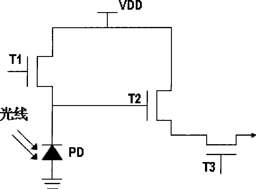
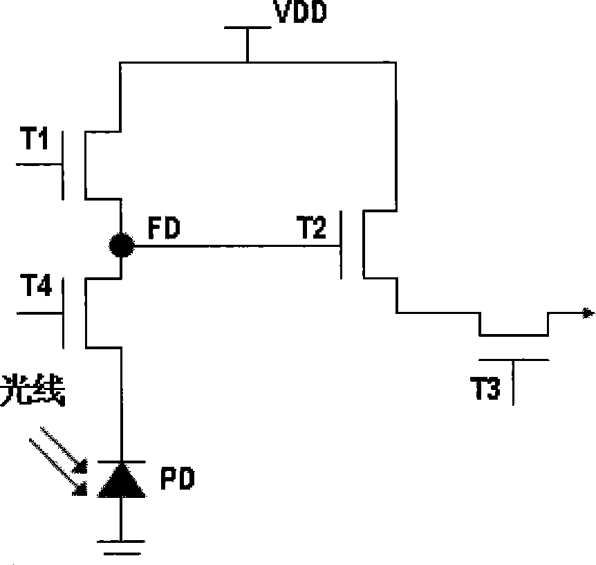
[0051] The following takes 3T-type pixels as an example to illustrate its implementation steps. image 3 A-A' cross-sectional view in a to illustrate, including steps:

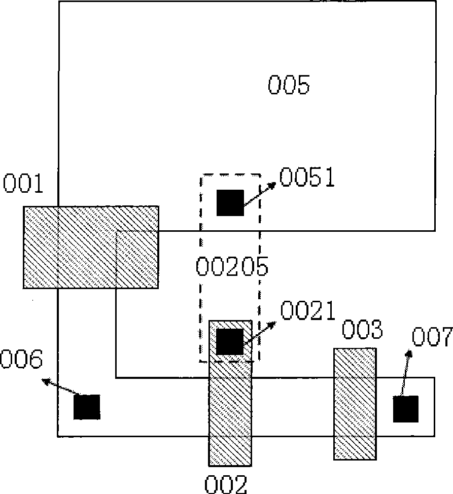
[0052] The first is the selection or preparation of SOI materials, Figure 4aThe SOI material structure is schematically shown, including a silicon substrate 01 , a buried oxide layer 02 and a silicon film 03 . The SOI material can be made by oxygen injection isolation technology (SIMOX, Seperation by Implantation of Oxygen), hydrogen injection bonding technology (Smart-Cut), oxygen injection bonding technology or common bonding technology. The silicon substrate 01 can be P-type silicon, or epitaxial P-type lightly doped silicon 01b on P-type heavily doped silicon 01a;

[0053] Such as Figure 4b As shown, the thickness of the epitaxial layer P-type silicon 01b is 1-10um, the doping concentration is 1E13-5E15, and the im...


PUM


Abstract

The invention discloses an SOI CMOS image sensor structure and a manufacturing method thereof. The manufacturing method comprises that: a CMOS image sensor is manufactured on an SOI material, and a photosensitive diode of the CMOS image sensor is manufactured in a silicon base of the SOI material; other devices of a CMOS circuit are manufactured on a silicon film; and the N pole and the P pole of the photosensitive diode are respectively led out by a metal plug and then connected with the CMOS circuit. The structure and the method not only has the advantages of high speed, low power consumption, lockout resistance and low probability of soft errors, but also make the light absorption efficiency of the photosensitive diode approximate to that of the bulk silicon CMOS sensor.

Description

technical field [0001] The invention relates to a CMOS image sensor, in particular to an SOI CMOS image sensor structure and a manufacturing method thereof. Background technique [0002] SOI (silicon-on-insulator) refers to silicon on the insulating layer, which is composed of three layers of "silicon film / insulating layer / silicon substrate". The uppermost silicon film (silicon film for short) is used to make semiconductor devices such as CMOS, and the intermediate insulating buried layer (usually silicon dioxide, referred to as buried oxide layer) is used to isolate the device from the silicon substrate. [0003] Compared with bulk silicon CMOS devices, SOI CMOS devices have the following advantages: small parasitic capacitance, low leakage, high speed and low power consumption; the common latch-up effect of bulk silicon CMOS is eliminated; the pulse current interference of the substrate is suppressed, and soft errors are reduced probability of occurrence. In terms of pro...

Claims


Application Information

Patent Timeline
Patent Type & Authority Applications(China)
IPC IPC(8): H01L27/146H01L21/8222H01L21/84H01L21/768
Inventor 高文玉陈杰旷章曲
Owner BEIJING SUPERPIX MICRO TECHNOLOGY CO LTD
Why Eureka
Try Eureka