

Planar superconducting microstrip resonator
A resonator and microstrip technology, applied in the field of resonators, can solve the problems of increasing the volume of the resonator, increasing the resonator, reducing the parasitic coupling, etc., and achieving the effect of compact overall area, small volume, and small electromagnetic radiation.
- Summary
- Abstract
- Description
- Claims
- Application Information
AI Technical Summary
Problems solved by technology
Method used
Image

Examples
no. 1 example
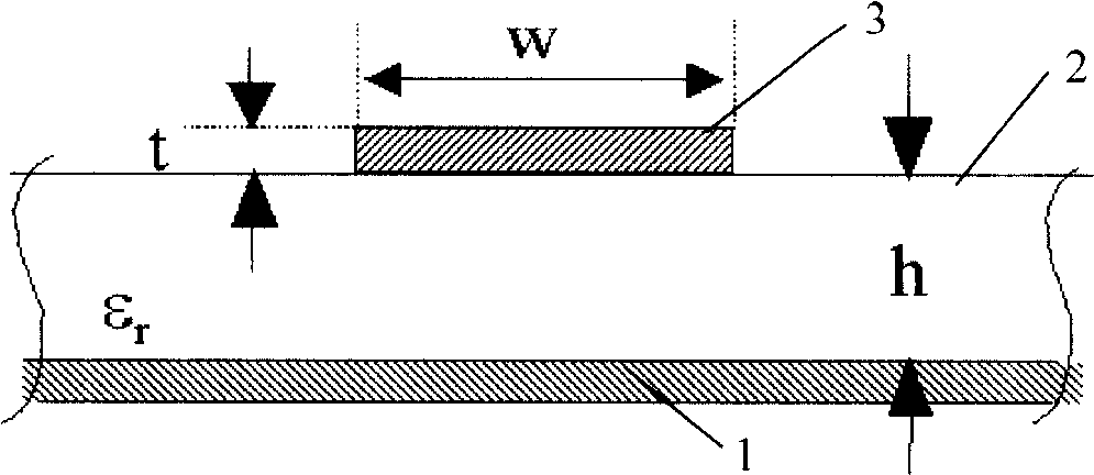
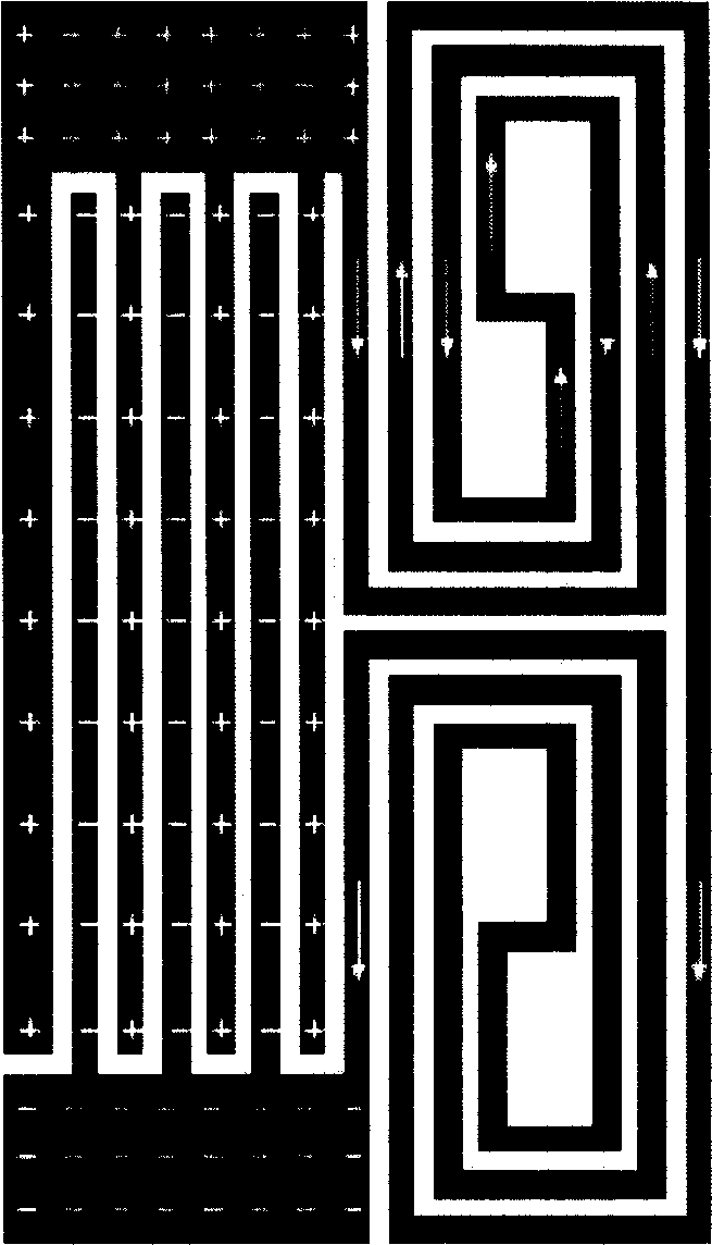
[0038] refer to figure 1 , 2 , using a complete microstrip line, the microstrip line is a superconducting microstrip line, the upper layer of the microstrip conductor 3 and the lower layer of the ground plane conductor 1 are high-temperature superconducting thin films, and the middle is a dielectric constant ε rsingle crystal dielectric sheet. Form a structure consisting of a set of finger capacitors, a set of double helix curve inductors connected in parallel, and then a set of block capacitors formed in series with the ground. In this embodiment, the selected microstrip line adopts the crystal medium LaAlO3, and its dielectric constant ε r =23.6, the block capacitor in this structure is selected as a rectangle, the finger capacitors are equal in length and width, and there are two double-helix inductors, which can minimize the volume of the resonator and maximize the use of space. The lines of the finger capacitors The curves of the double-helix inductor and the double-he...
no. 2 example
[0047] A complete superconducting microstrip line is used to form a structure consisting of a set of finger capacitors, a set of double helix curve inductors connected in parallel, and then a set of block capacitors formed in series with the ground. In this embodiment, the straight line of the bulk capacitor, the equal length, equal width and equal distance of the interpolated capacitor, the interpolated capacitor line is a broken line, the double helical inductance has three turns, and the curves of the double helical inductance are all equal in width and equidistant, such as Figure 3b shown.
[0048] In this embodiment, the maximum side length of the outer ring is 6.4 mm, the maximum side width is 5.2 mm, the line width of the microstrip line is 0.4 mm, the distance between the inner and outer ring lines is 0.3 mm, and the distance between the opening ends of the inner and outer rings is 0.12 mm.
no. 3 example
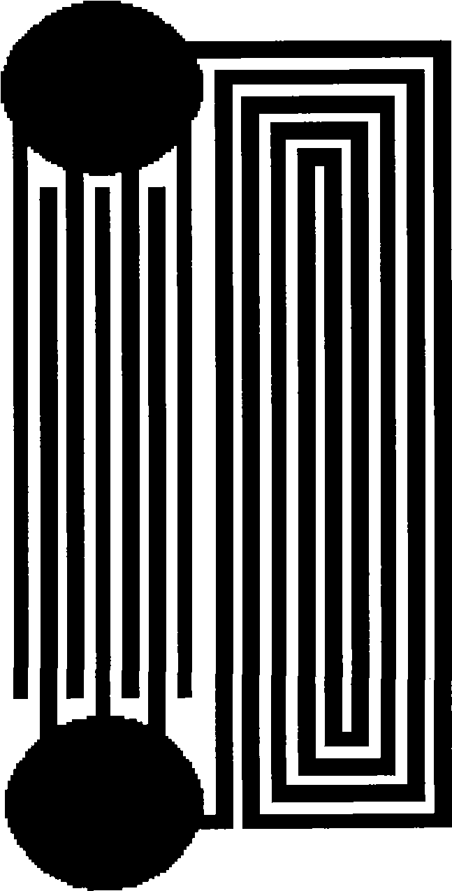
[0050] A complete superconducting microstrip line is used to form a structure consisting of a set of finger capacitors, a set of double helix curve inductors connected in parallel, and then a set of block capacitors formed in series with the ground. In this embodiment, the block capacitors are selected as triangles, the finger capacitors have different lengths and widths, and there are two double-helical inductors, and the curves of the double-helical inductors are all unequal widths and different distances.
[0051] In this embodiment, the maximum side length of the outer ring is 6.0 mm, the maximum side width is 5.2 mm, the line width of the microstrip line is 0.5 mm, the distance between the inner and outer ring lines is 0.3 mm, and the distance between the opening ends of the inner and outer rings is 0.12 mm.
PUM
| Property | Measurement | Unit |
|---|---|---|
| Line width | aaaaa | aaaaa |
Abstract
Description
Claims
Application Information