Package process of light emitting element

A light-emitting element and packaging process technology, applied in the direction of electrical components, semiconductor/solid-state device manufacturing, electric solid-state devices, etc., can solve the problems of process bottlenecks, limitations, secondary processing of external circuits, etc., to improve luminous efficiency and reduce manufacturing costs. Cost, the effect of increasing production capacity

Inactive Publication Date: 2009-10-07
LIUNG FENG INDAL
View PDF0 Cites 6 Cited by
  • Summary
  • Abstract
  • Description
  • Claims
  • Application Information

AI Technical Summary

Problems solved by technology

However, the light-emitting diode chip must be electrically connected to the external circuit through the electrodes on it to be able to emit light. Therefore, in the manufacturing process of the aforementioned light-emitting element, a contact point that can be electrically connected must be reserved at the electrode. Leaving steps not only creates a bottleneck in the process, but also causes secondary processing operations that are necessary when connecting external circuits
[0003] Furthermore, in the structure of the existing light-emitting element, the light-emitting diode chip is bonde

Method used


Image

  • Package process of light emitting element
  • Package process of light emitting element
  • Package process of light emitting element

Examples


no. 1 example

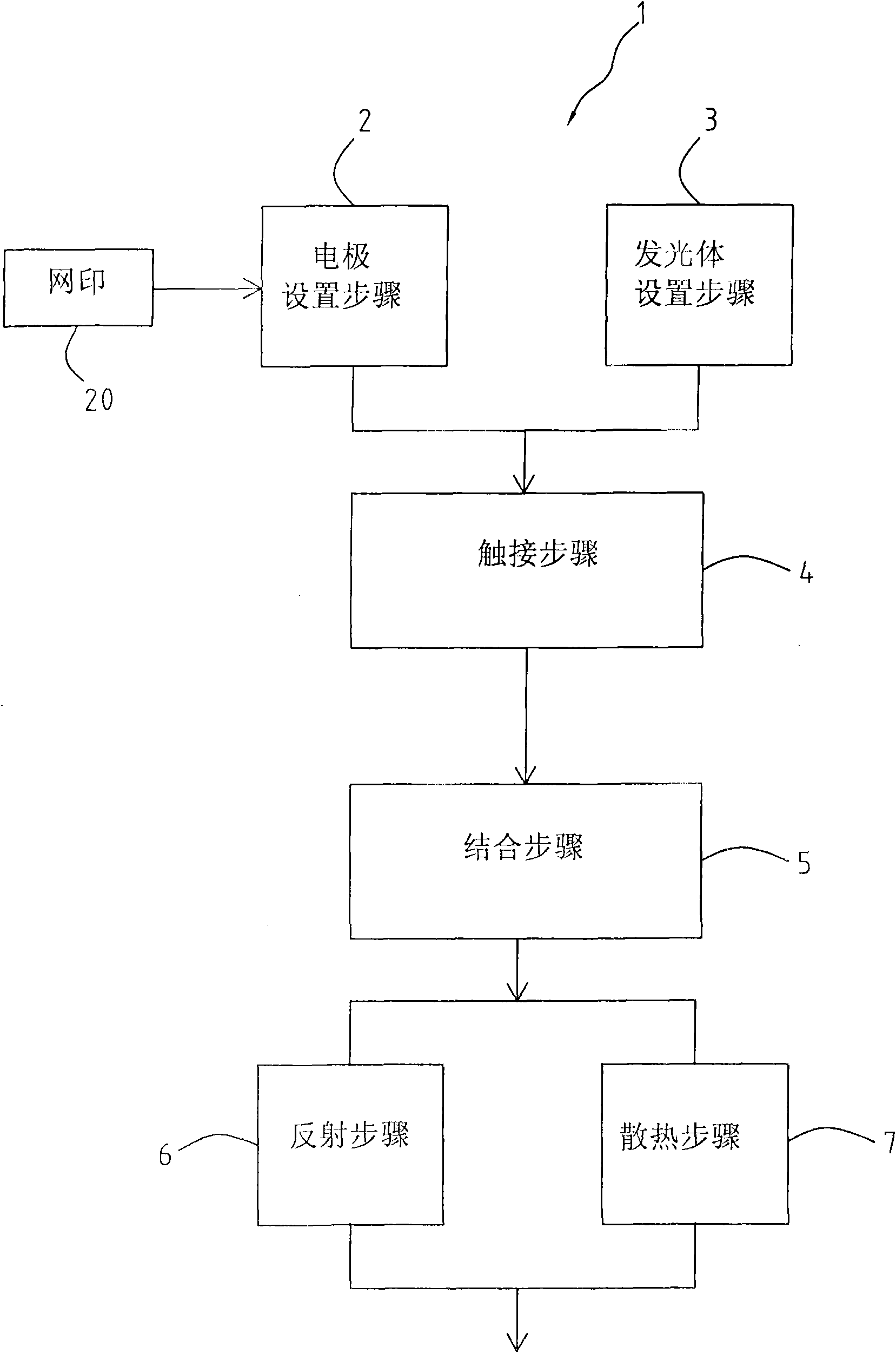
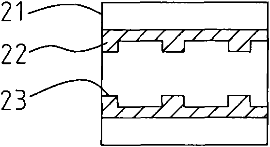
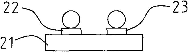
[0021] Refer to Figure 2A -F is the first embodiment of the packaging process of the light-emitting element of the present invention. In this embodiment, a positive electrode 22 and a negative electrode 23 are defined by etching on a carrier 21, so that the carrier 21 is formed with a positive electrode and a negative electrode Electrode slide (that is, step 2 of electrode setting, refer to Figure 2A and Figure 2B As mentioned above, the material of the positive electrode and the negative electrode can also be directly selected in the actual operation to directly define the electrode, or the electrode carrier sheet that has the positive electrode and the negative electrode can be selected without going through the etching process), in addition, Select a surface mount (SMD) light-emitting diode chip 31, which has a positive electrode 32 and a negative electrode 33 (that is, the light-emitting body setting step 3), and then define the positive electrode by ball grid array packagi...


PUM


Abstract

The invention relates to a package process of a light emitting element, comprising: an electrode setting step, an illuminant setting step, a contact step and a combining step. In the electrode setting step, a anode and a cathode are defined; in the illuminant setting step, a light emitting diode wafer having an anode and a cathode is used as an illuminant ; in the contact step, the defined anode and the cathode as well as the anode and the cathode on the light emitting diode wafer are communicated and combined into a whole; and in the combining step, the defined anode and the cathode and the light emitting diode wafer are tightly combined into a whole. In the package process of the light emitting element, the electrode of the light emitting diode wafer can be communicated with an outside electrode in advance, thereby work for assembling posterior-segment products can be simplified, the productivity can be increased, and the production cost can be reduced.

Description

Technical field [0001] The present invention relates to a packaging process for a light-emitting element, in particular to a process for manufacturing a light-emitting element with a light-emitting diode chip. The method can increase productivity and reduce manufacturing costs, and can make the manufactured light-emitting element The luminous efficiency is improved. Background technique [0002] In the prior art production of light-emitting elements with light-emitting diode chips, the light-emitting diode chips are first manufactured, and then the light-emitting diode chips are fixed in a base with a recessed portion by a bonding material, and the When the recess is filled, the manufacture of the light-emitting element is completed. However, the light-emitting diode chip must be electrically connected to an external circuit through its electrodes to be able to emit light. Therefore, in the manufacturing process of the aforementioned light-emitting element, a contact point that c...

Claims


Application Information

Patent Timeline
IPC IPC(8): H01L33/00H01L21/60H01L23/488
CPCH01L24/17H01L2224/48091H01L2224/16225H01L2224/48227H01L2224/17H01L2924/12041H01L2924/00014H01L2924/00H01L2924/00012
Inventor 许苍林林恒毅
Owner LIUNG FENG INDAL
Why Eureka
Try Eureka