Array substrate of liquid crystal display device

A technology of a liquid crystal display device and an array substrate, which is applied in the field of array substrates, and can solve the problems of high step difference between the data line area and the pixel area, and high anti-friction resistance, and achieve the effects of reducing resistance, improving quality, and overcoming the phenomenon of poor friction

Active Publication Date: 2009-10-21
K TRONICS (SUZHOU) TECH CO LTD +1
View PDF1 Cites 18 Cited by
  • Summary
  • Abstract
  • Description
  • Claims
  • Application Information

AI Technical Summary

Problems solved by technology

[0004] The purpose of the present invention is to provide a liquid crystal display device, which solves the defect that the step difference between the data line area and the pixel area in the prior art is too high, and realizes a liquid crystal display device with high anti-friction resistance

Method used


Image

  • Array substrate of liquid crystal display device
  • Array substrate of liquid crystal display device
  • Array substrate of liquid crystal display device

Examples


no. 1 example

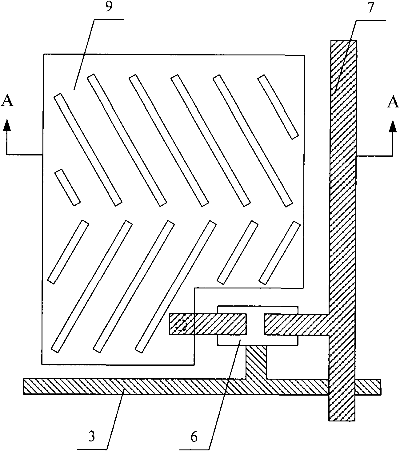
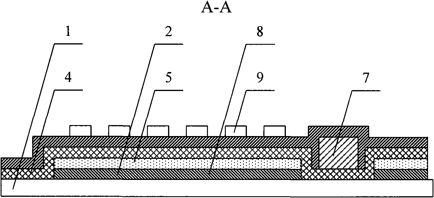
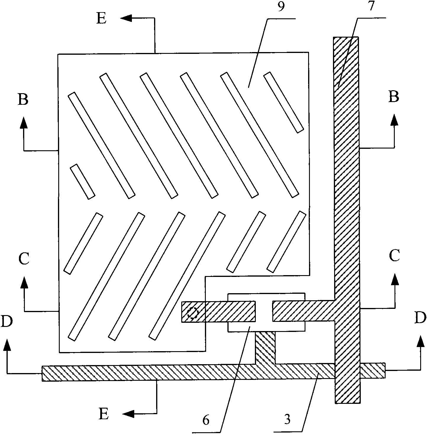
[0031] Figure 1a is a schematic structural view of the first embodiment of the array substrate of the liquid crystal display device of the present invention, Figure 1b for Figure 1a Schematic diagram of the A-A section in the middle, such as Figure 1a with Figure 1b As shown, the specific structure of the array substrate of the liquid crystal display device of the present invention includes: a substrate 1, a gate line 3 located on the substrate 1, a data line 7 crossing the gate line 3, a thin film transistor electrically connected to the gate line 3 and the data line 7 , and the pixel electrode 9 electrically connected to the thin film transistor is located in the area defined by the intersection arrangement of the gate line 3 and the data line 7, a common electrode 5 is provided under the gate insulating layer 4, and a passivation layer 8 is provided above the data line 7, The active layer 6 is located between the gate electrode (the electrode branched from the gate lin...


PUM


Abstract

The invention relates to an array substrate of a liquid crystal display device, comprising a substrate, a grid line arranged on the substrate, a data wire intersected with the grid line, a thin film transistor which is electrically connected with the grid line and the data wire, and a pixel electrode which is electrically connected with the thin film transistor and positioned in an area defined by a crossed array of the grid line and the data wire; a section difference supplementation layer is arranged between the substrate and the grid line; and the section difference supplementation layer which corresponds to the data wire is provided with a first groove. By the first groove arranged on the section difference supplementation layer, the array substrate reduces the height of the data wire area and ensures that the height of the data wire area is equal to the height of the pixel area, thereby overcoming the defect of unfavorable friction of an oriented film on the surface of the prior array substrate.

Description

technical field [0001] The invention relates to an array substrate of a liquid crystal display device, in particular to an array substrate of a liquid crystal display device with high rubbing resistance. Background technique [0002] A liquid crystal display device is a main flat display device. With the technical progress of the liquid crystal display device, the performance of the liquid crystal display device is gradually improved, such as viewing angle performance, contrast ratio, response performance and the like. Now, in order to meet higher display requirements, the driving mode of the liquid crystal display device has been increased from 60Hz to 120Hz. The 60Hz driving method is a display method of refreshing 60 pictures per second, and the 120Hz driving method is a display method of refreshing 120 pictures per second. This method can improve the display effect of the liquid crystal display device. However, with the resistance of the current gate lines and data lin...

Claims


Application Information

Patent Timeline
Patent Type & Authority Applications(China)
IPC IPC(8): G02F1/1362H01L27/12
Inventor 闵泰烨邱海军王章涛赵继刚
Owner K TRONICS (SUZHOU) TECH CO LTD
Why Eureka
Try Eureka