
Semiconductor encapsulation structure by taking lead frame as substrate and applicable lead frame thereof

A lead frame and semiconductor technology, applied in the field of lead frame, can solve problems such as the inclination or displacement of the chip 140, the length of the first pin 110 cannot be shortened, and the structural strength of the chip 140 cannot be provided, so as to strengthen the chip load strength and increase the chip load The effect of strength and strengthening the locking ability

Inactive Publication Date: 2009-10-21
POWERTECH TECHNOLOGY
View PDF0 Cites 4 Cited by
  • Summary
  • Abstract
  • Description
  • Claims
  • Application Information

AI Technical Summary

Problems solved by technology

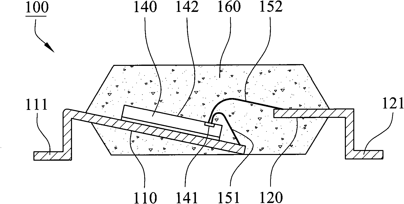
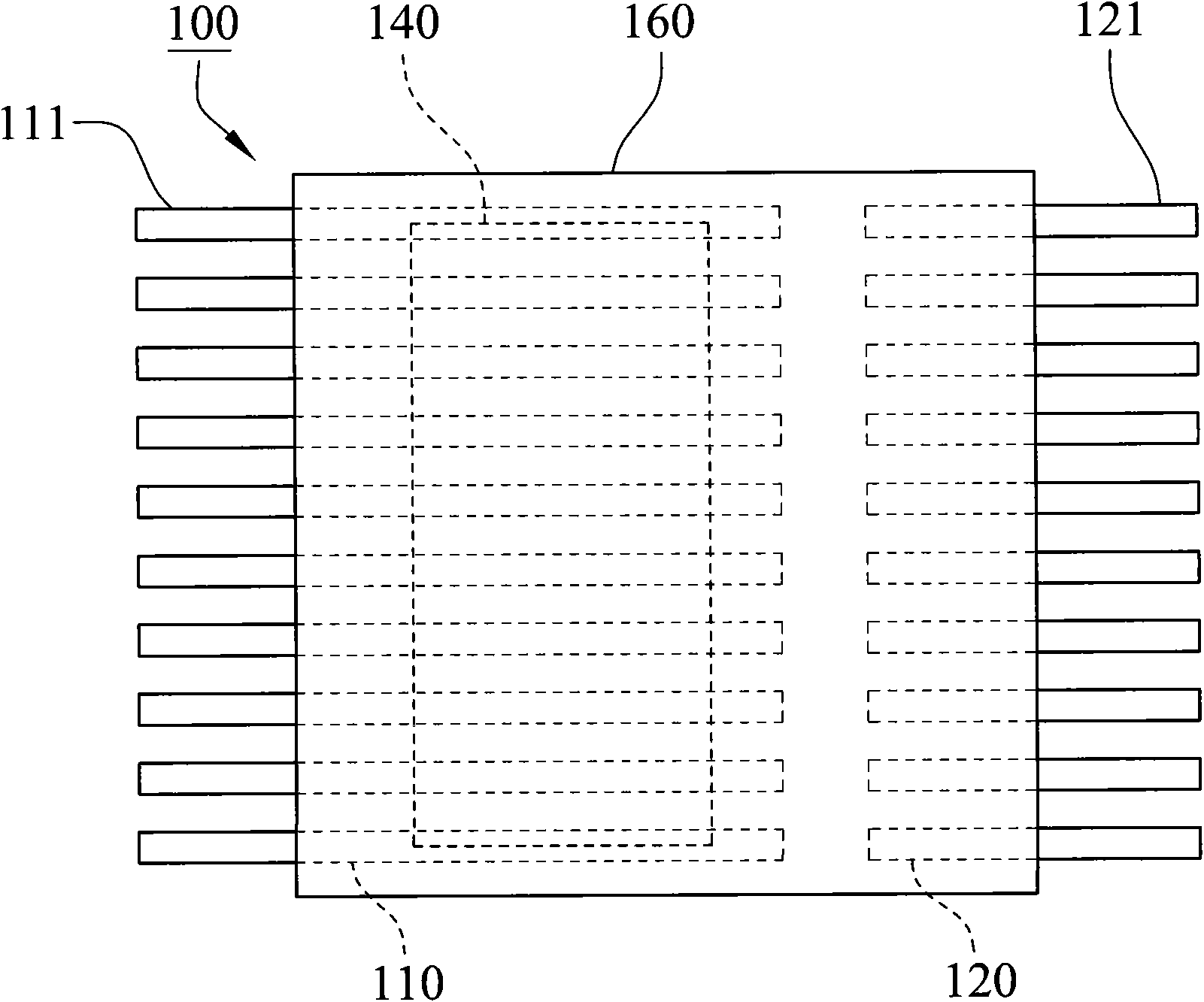
[0004] However, if figure 1 As shown, the semiconductor package structure 100 is only carried on the first pins 110 on one side of the lead frame, and the length of the first pins 110 cannot be shortened, and the structural strength enough to carry the chip 140 cannot be provided.
During the potting process of forming the encapsulant 160 , the chip 140 is likely to be tilted or displaced due to mold flow pressure, which may even cause improper alignment of the first pins 110 , the chip 140 or the first bonding wires 151 Exposed, resulting in failure of semiconductor packaging products

Method used


Image

  • Semiconductor encapsulation structure by taking lead frame as substrate and applicable lead frame thereof
  • Semiconductor encapsulation structure by taking lead frame as substrate and applicable lead frame thereof
  • Semiconductor encapsulation structure by taking lead frame as substrate and applicable lead frame thereof

Examples


Embodiment Construction

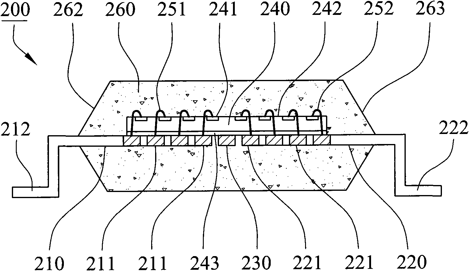
[0045] According to a specific embodiment of the present invention, a semiconductor package structure based on a lead frame and an applicable lead frame are disclosed. see image 3 and Figure 4As shown, the semiconductor package structure 200 mainly includes at least one first lead 210, at least one second lead 220, connection bar 230, chip 240, two or more first bonding wires 251, two or two The second bonding wire 252 and the encapsulant 260 above. The semiconductor package structure 200 has a chip-on-lead (COL, Chip-On-Lead) package structure.

[0046] like Figure 5 and Image 6 As shown, the first pin 210, the second pin 220 and the connection bar 230 form the same lead frame, including the same metal material, generally made of copper or iron metal, and have an appropriate thickness (about 0.2mm) . Each first pin 210 has a first finger 211 , and each second pin 220 has a second finger 221 . The connecting bar 230 is disposed between the first pin 210 and the seco...


PUM


Abstract

The invention discloses a semiconductor encapsulation structure by taking a lead frame as a substrate and the applicable lead frame thereof. The semiconductor encapsulation structure mainly comprises at least one first pin, at least one second pin and a connecting strip which is arranged between the first pin and the second pin of the lead frame and also comprises a chip, two or more weld lines and an adhesive body which are arranged on the first pin, the second pin and the connecting strip, wherein the chip is provided with two or more weld pads, and the weld pads are connected to a first finger joint of the first pin and a second finger joint of the second pin by the weld lines; the connecting strip is provided with an extending part which exceeds the first finger joint of the first pin and the second finger joint of the second pin and is connected to the side of the adhesive body, and the extending part forms an arch for blocking stress transfer and preventing a crack being formed in such a way that drag stress is directly transferred in a bonded wafer area from the side of the adhesive body when the connecting strip is sheared, and the delamination of the connecting strip due to hydrosphere invasion along the crack of the connecting strip is avoided.

Description

technical field [0001] The present invention relates to a semiconductor device, in particular to a semiconductor package structure based on a leadframe and the applicable leadframe. Background technique [0002] Although in the field of semiconductor packaging, printed circuit boards or other substrates have gradually replaced lead frames as chip carriers, semiconductor package structures based on lead frames still have the advantages of low cost and high durability. One of the package structures is chip On the pin (COL, Chip-On-Lead), which is to set the semiconductor chip on a plurality of pins of the lead frame, use the bonding wire formed by the wire as the internal electrical connection between the chip and the pin, and pass The mold encapsulation enables the encapsulant to cover the chip and the bonding wire, and the exposed pins on the side of the encapsulant are used as external electrical connections. Although chip-on-lead (COL) semiconductor packaging construction...

Claims


Application Information

Patent Timeline
Patent Type & Authority Applications(China)
IPC IPC(8): H01L23/488H01L23/31H01L23/495
CPCH01L2224/48091H01L2224/48247H01L2224/48257H01L2224/49109H01L2224/73265
Inventor 王进发谢宛融徐玉梅
Owner POWERTECH TECHNOLOGY
Learn More