Doping method and method for forming LDD doped area

A technology of doping regions and point defects, which is applied in the field of doping methods and the formation of LDD doping regions, can solve the problems of deep junctions and achieve the effect of reducing junction depths

Inactive Publication Date: 2009-11-11
SEMICONDUCTOR MANUFACTURING INTERNATIONAL (BEIJING) CORP
View PDF1 Cites 7 Cited by
  • Summary
  • Abstract
  • Description
  • Claims
  • Application Information

AI Technical Summary

Problems solved by technology

[0006] The invention provides a doping method and a method for forming an LDD doped region, so as to solve the problem that the junction depth formed by the existing LDD implantation process is relatively deep

Method used


Image

  • Doping method and method for forming LDD doped area
  • Doping method and method for forming LDD doped area
  • Doping method and method for forming LDD doped area

Examples


Embodiment Construction

[0035] The specific embodiments of the present invention will be described in detail below in conjunction with the accompanying drawings.

[0036] With the continuous improvement of the semiconductor integrated circuit manufacturing process, the line width of the gate is getting smaller and smaller, and correspondingly, the junction depth of the doped region is also required to be shallower. The invention provides a doping method capable of forming a doped region with a shallower junction depth.

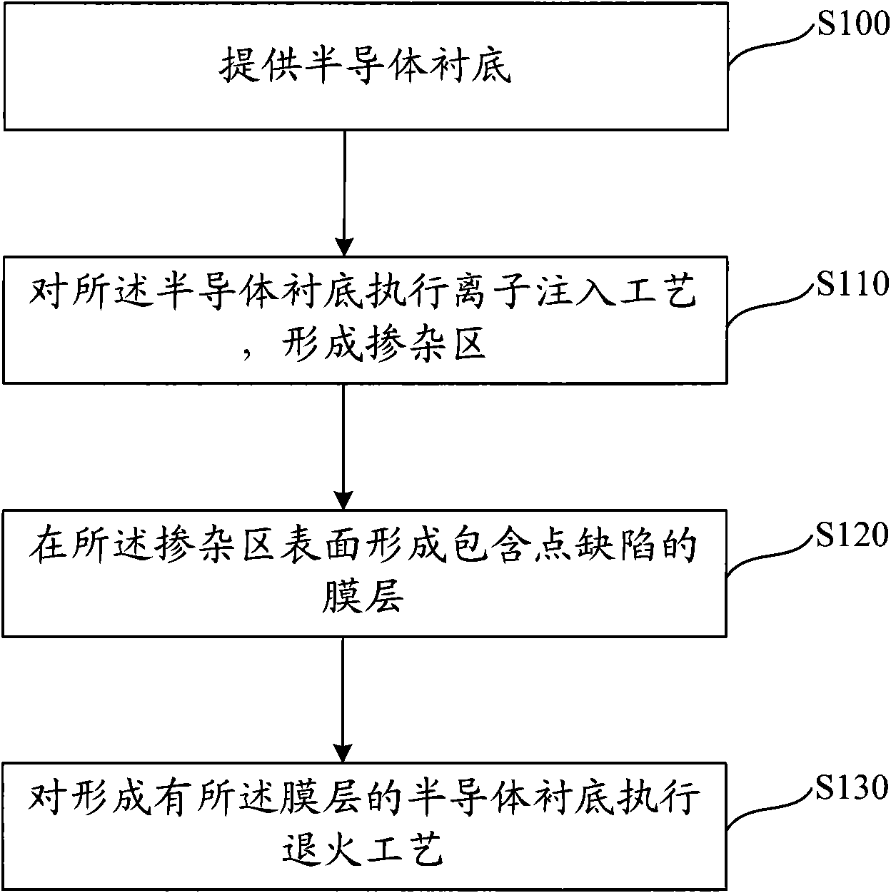
[0037] figure 1 It is a flowchart of an embodiment of the doping method of the present invention.

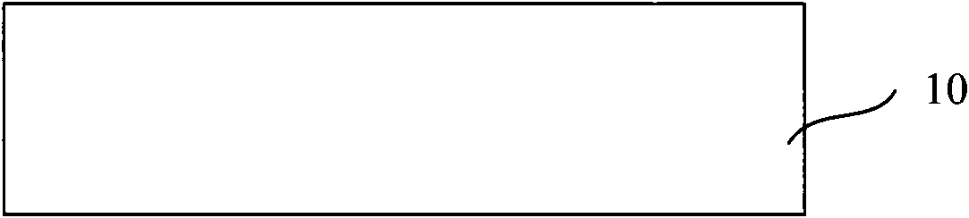
[0038] Please refer to figure 1 , step S100 is to provide a semiconductor substrate.

[0039] Step S110 is performing an ion implantation process on the semiconductor substrate to form a doped region.

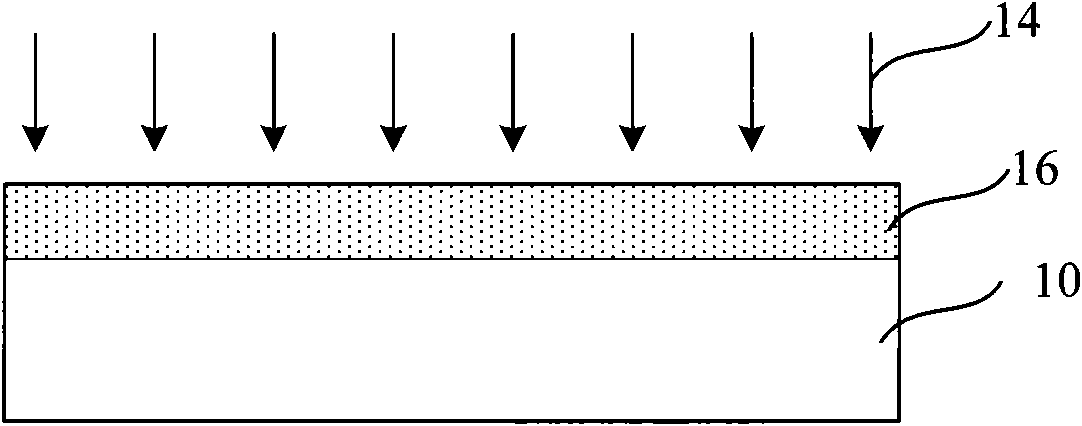
[0040] Step S120 is forming a film layer containing point defects on the surface of the doped region.

[0041] Step S130 is performing an annealing process on the semiconductor sub...


PUM


Abstract

The invention relates to a doping method comprising the following steps: providing a semiconductor substrate; processing the semiconductor substrate with an ion injection process to form a doped area; forming a film containing point defect on the surface of the doped area; and processing the semiconductor substrate with the film formed thereon with an anneal process. The invention also provides a method for forming an LDD doped area. The junction depth of the doped area formed in the invention is shallower.

Description

technical field [0001] The invention relates to the technical field of semiconductor manufacturing, in particular to a doping method and a method for forming an LDD doping region. Background technique [0002] With the continuous development of complementary metal-oxide-semiconductor transistor manufacturing technology, the integration level is getting higher and higher, the line width of the gate is getting smaller and smaller, and the length of the conductive channel under the gate is also continuously decreasing. [0003] In order to avoid or suppress the leakage current between the source and the drain caused by the shortening of the conductive channel length, the industry introduces a light doped drain (LDD) implantation process, that is, the source and drain are heavily doped Previously, shallow junction implants were performed with ions of higher molecular weight. [0004] In the Chinese patent application document with publication number CN 1983529A, a method for LD...

Claims


Application Information

Patent Timeline
Patent Type & Authority Applications(China)
IPC IPC(8): H01L21/265H01L21/336
Inventor 林仰魁
Owner SEMICONDUCTOR MANUFACTURING INTERNATIONAL (BEIJING) CORP
Why Eureka
Try Eureka