Buffer based on source electrode follower

A source follower and buffer technology, applied in amplifiers with impedance circuits, logic circuits using dielectric elements, logic circuits using specific components, etc., can solve the problem of large analog input signal loss, small signal gain, Problems such as poor dynamic performance, to achieve the effect of high unity gain buffer output

Inactive Publication Date: 2009-12-02
INST OF MICROELECTRONICS CHINESE ACAD OF SCI
View PDF0 Cites 22 Cited by
  • Summary
  • Abstract
  • Description
  • Claims
  • Application Information

AI Technical Summary

Problems solved by technology

[0009] In order to solve the problems of existing high-speed buffer signal gain less than 1, large analog input signal loss

Method used


Image

  • Buffer based on source electrode follower
  • Buffer based on source electrode follower
  • Buffer based on source electrode follower

Examples


Embodiment 1

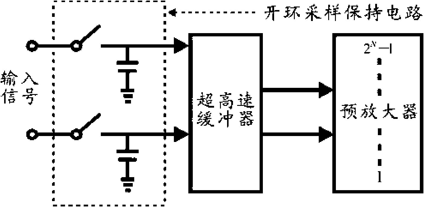
[0032] see Figure 4 , an embodiment of the present invention provides a buffer based on a source follower, the buffer includes:

[0033] a pseudo-differential input stage for receiving a differential input signal;

[0034] A cross-coupled common-source stage connected to a pseudo-differential input stage to form a negative resistance to cancel out the output resistance of the buffer;

[0035] a current source coupled to the pseudo-differential input stage for providing buffer branch current;

[0036] A capacitive load, connected to the pseudo-differential input stage, is used as an output load for the buffer.

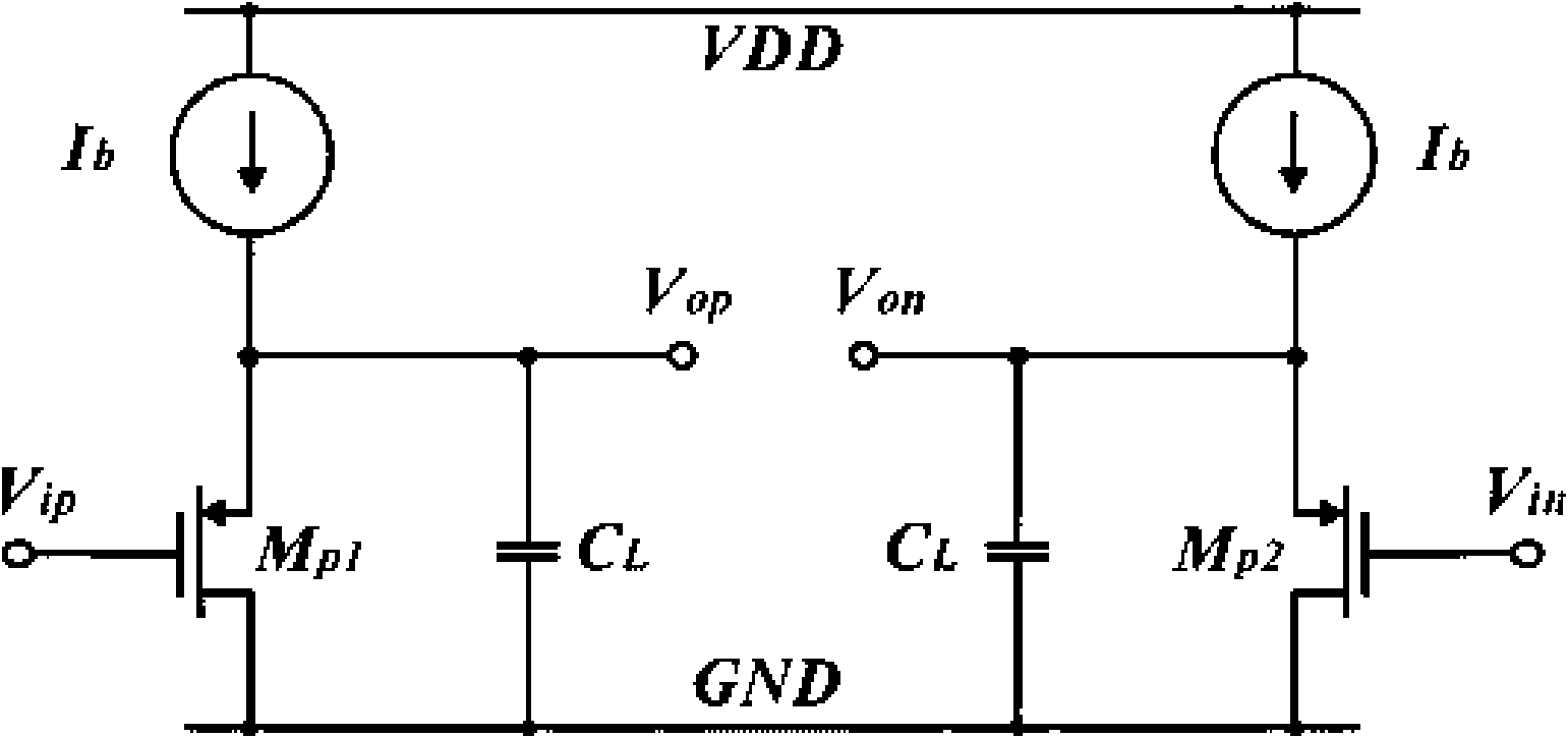
[0037] Wherein, the pseudo-differential input stage includes a first PMOS transistor 110 (Mp1) and a second PMOS transistor 111 (Mp2); the drain of the first PMOS transistor 110 is connected to the ground voltage GND (141), and the gate of the first PMOS transistor 110 is connected to the second PMOS transistor 110. An input terminal 102 (Vip), the source and substr...

Embodiment 2

[0043] see Figure 5 , the embodiment of the present invention also provides another buffer based on a source follower, and the buffer includes:

[0044] a pseudo-differential input stage for receiving a differential input signal;

[0045]A cross-coupled common-source stage connected to a pseudo-differential input stage to form a negative resistance to cancel out the output resistance of the buffer;

[0046] a current source coupled to the pseudo-differential input stage for providing buffer branch current;

[0047] A capacitive load, connected to the pseudo-differential input stage, is used as an output load for the buffer.

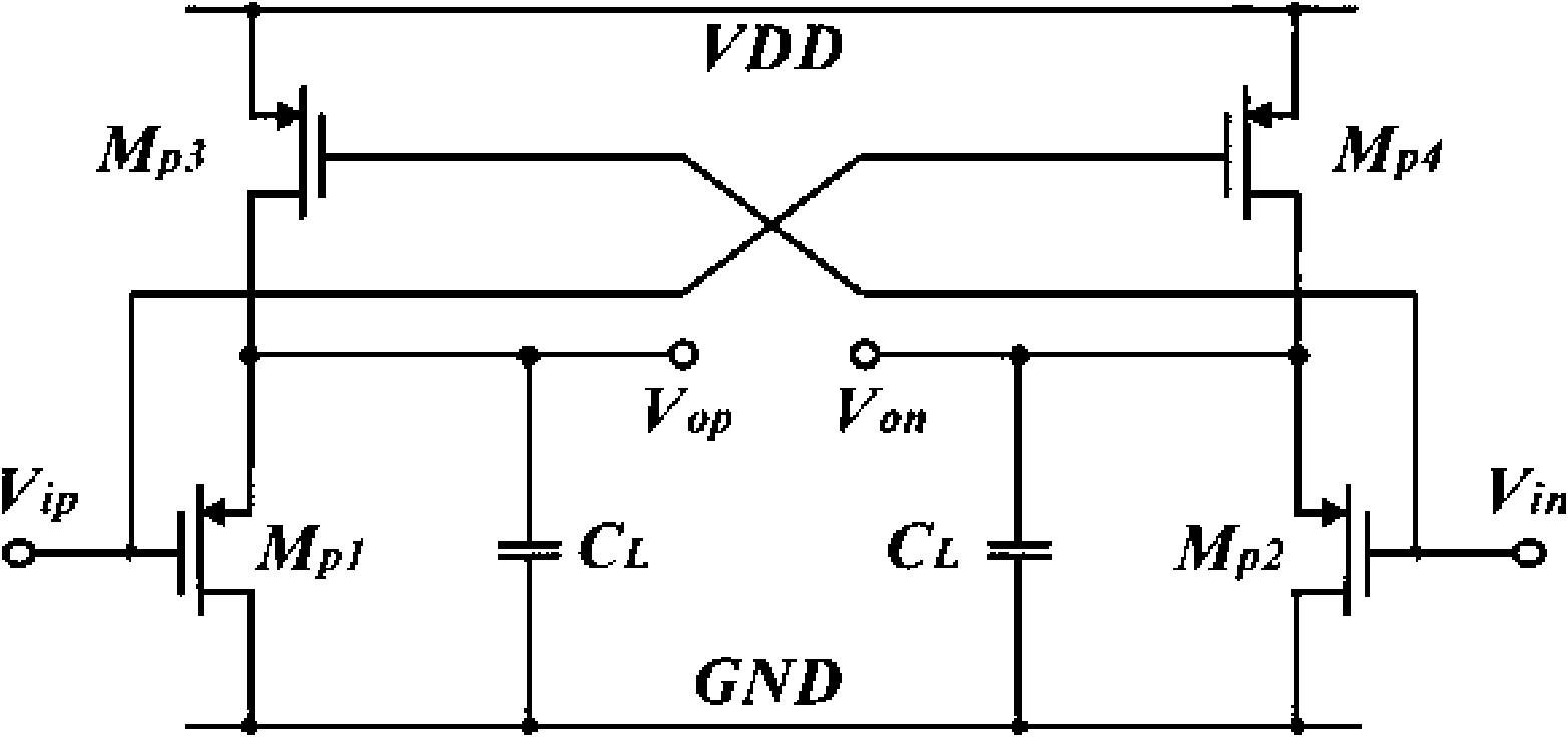
[0048] Wherein, the pseudo-differential input stage includes a first PMOS transistor 210 (Mp1) and a second PMOS transistor 211 (Mp2); the drain of the first PMOS transistor 210 is connected to the ground voltage GND (241), and the gate of the first PMOS transistor 210 is connected to the second PMOS transistor 210. An input terminal 202 (Vip), the so...


PUM


Abstract

The invention discloses a buffer based on a source electrode follower and belongs to the technical field of analog integrated circuit design. The buffer comprises a pseudo differential input level, a cross coupling common source level, a current source and a capacitance load, wherein the pseudo differential input level is used for receiving a difference input signal; the cross coupling common source level is connected with the pseudo differential input level, used for forming negative resistance and offsetting output resistance of the buffer; the current source is connected with the pseudo differential input level and used for providing branch current of the buffer; and the capacitance load is connected with the pseudo differential input level and used as output load of the buffer. The negative resistance is formed by the cross coupling common source level, so that the buffer offsets the output resistance of the high-speed buffer and realizes unity-gain buffering output. The buffer based on the source electrode follower realizes ultra-high speed, the unity-gain buffering output and high dynamic characteristics by theoretical analysis and simulation verification.

Description

technical field [0001] The invention relates to the technical field of analog integrated circuit design, in particular to a buffer based on a source follower. Background technique [0002] The all-parallel analog-to-digital converter (flash ADC) is the fastest conversion speed among various types of analog-to-digital converters, and it is mainly used in the field of data acquisition with low precision and ultra-high speed (sampling frequency greater than 1GHz). figure 1 A schematic diagram of an analog front-end circuit of an all-parallel analog-to-digital converter is shown, which mainly includes an open-loop sample-and-hold circuit, an ultra-high-speed buffer and a pre-amplifier. Usually, since the fully parallel analog-to-digital converter needs to process the input analog signal in parallel, it also requires 2 N -1 pre-amplifier is connected in parallel to increase the input capacitance, therefore, it is necessary to add a super high-speed buffer at the output of the op...

Claims


Application Information

Patent Timeline
IPC IPC(8): H03K19/185H03F3/50
Inventor 陈勇周玉梅
Owner INST OF MICROELECTRONICS CHINESE ACAD OF SCI
Why Eureka
Try Eureka