Implementation method of multi-defective one-dimensional photonic crystal all-optical switch with stable and controllable output state

A technology of dimensional photonic crystal and output state, applied in optics, nonlinear optics, instruments, etc., can solve the problems that all-optical switching cannot be realized, and the transmission state of photonic crystal cannot be stabilized.

Inactive Publication Date: 2009-12-09
BEIJING UNIV OF POSTS & TELECOMM
View PDF0 Cites 9 Cited by
  • Summary
  • Abstract
  • Description
  • Claims
  • Application Information

AI Technical Summary

Problems solved by technology

If Δn cannot be a constant value, that is, the transmission state of the photonic crystal cannot be stable, and the all-optical switch cannot be realized.

Method used


Image

  • Implementation method of multi-defective one-dimensional photonic crystal all-optical switch with stable and controllable output state
  • Implementation method of multi-defective one-dimensional photonic crystal all-optical switch with stable and controllable output state
  • Implementation method of multi-defective one-dimensional photonic crystal all-optical switch with stable and controllable output state

Examples


Embodiment

[0041] Implementation example: a method for realizing a multi-defect one-dimensional photonic crystal all-optical switch with a stable and controllable output state near a wavelength of 1550nm.

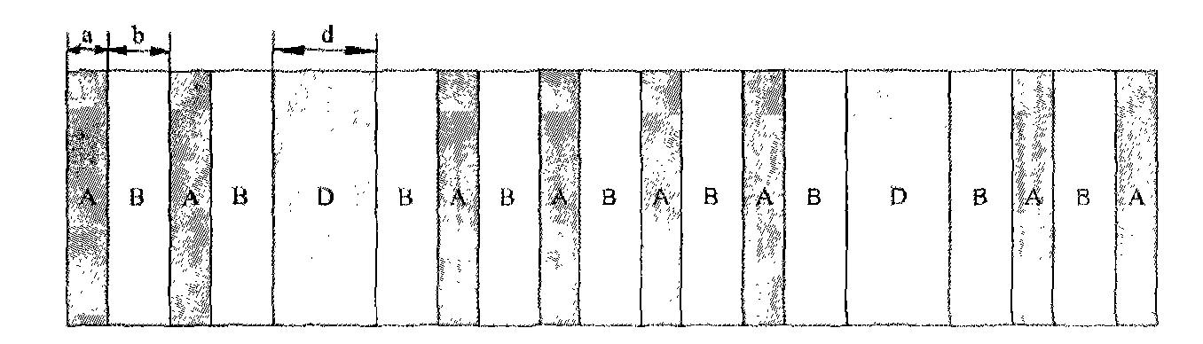
[0042] Select TiO with higher third-order nonlinear susceptibility 2 As the material of the nonlinear defect layer D layer, the linear part of the refractive index of the medium is n d0 =2.5, the nonlinear refractive index coefficient is -6.32×10 -10 cm 2 / kW. Layer A is made of commonly used semiconductor material Si, with a refractive index of n a =3.5; Layer B is air. a, b, and d are the thicknesses of the corresponding layers, satisfying a*n a =b*n b =λ 0 / 4, d=λ 0 / 2 / 2.5; lambda 0 =1550nm, ω 0 = 2πc / λ 0 .

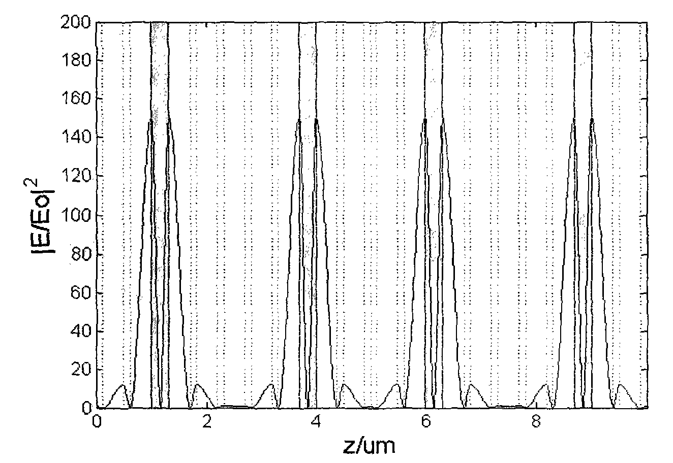
[0043] Pump light frequency ω p = ω 0 , light intensity I P = I 0 =10 4 kW / cm 2 ; signal light frequency ω s =1.029644ω 0 , the light intensity is much smaller than the pump light intensity.

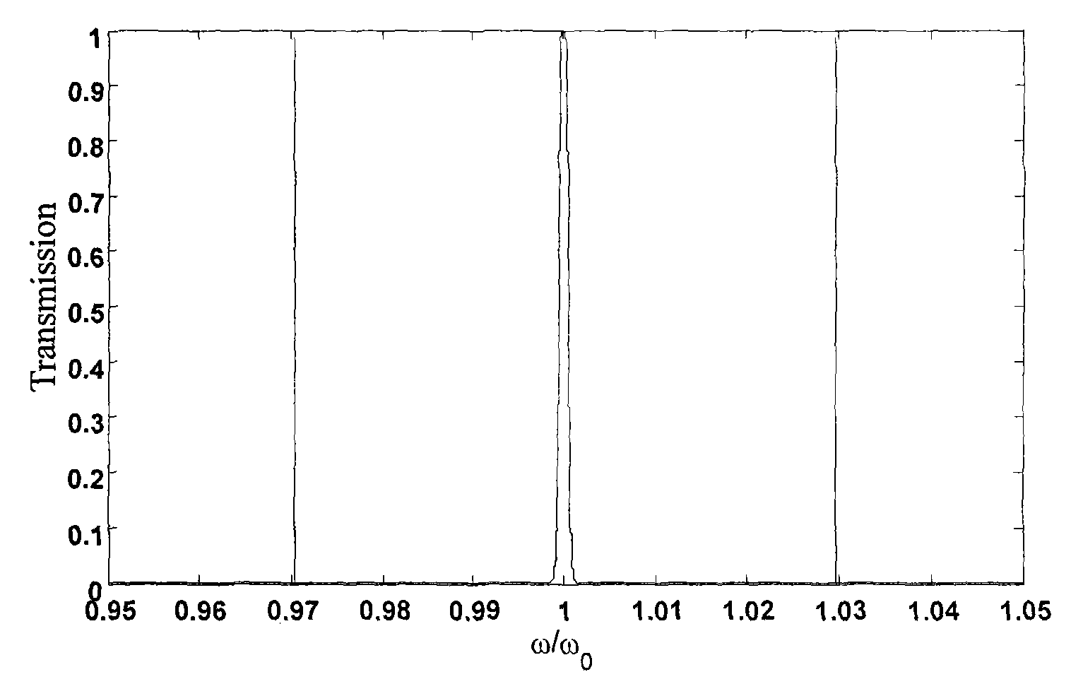
[0044] When the pump light intensity is 0, the transmission spe...


PUM

PropertyMeasurementUnit
refractive indexaaaaaaaaaa
transmittivityaaaaaaaaaa
refractive indexaaaaaaaaaa

Abstract

The invention relates to an implementation method of a multi-defective one-dimensional photonic crystal all-optical switch with stable and controllable output state; the invention designs a one-dimensional photonic crystal cascade structure, a nonlinear material having higher nonlinear coefficient is added into a linear dielectric layer arrayed periodically, optical switch effect is realized by a broadband detect mode and a narrowband defect mode caused by introducing a multi-defect structure, and the stable control of pump light on the refractive index of a nonlinear medium is realized and the problem that the output state is difficult to be steadily controlled existing in the all-optical switch design is solved simultaneously, thus obtaining the all-optical switch realizing stable performance and quick response time, and providing the method for realizing the all-optical switch for fields such as future all-optical communication networks, optical computers and the like.

Description

technical field [0001] The invention relates to a method for realizing a multi-defect one-dimensional photonic crystal all-optical switch with stable and controllable output states, belonging to the technical field of all-optical switches. Background technique [0002] As one of the key devices to realize the future all-optical network, the all-optical switch has become a research hotspot in recent years. So far, research on all-optical switches has mainly focused on semiconductors (Reference 1, Hirohito Yamada, Tao Chu, Makoto Tojo, Shigeru Nakamura, Masatoshi Tokushima, Yutaka rino, Satomi Ishida and Yasuhiko Arakawa. A compact optical switch module with Si-wire waveguides. 2007 IEEE. and Document 2, TEIXEIRA A, SILVEIRAT, et al. All-Optical Switching With SOA Based Devices. Advanced Optoelectronics andlasers, 2005.2005, (1): 52-55), Optical Fiber (Document 3, Yokota, H. Kobayashi, M. Mineo, H. Kagawa, N. Kanbe, H. Sasaki, Y. Demonstration of an all-optical switching op...

Claims


Application Information

Patent Timeline
Patent Type & Authority Applications(China)
IPC IPC(8): G02F1/35
Inventor 田慧平王博刘彬纪越峰
Owner BEIJING UNIV OF POSTS & TELECOMM
Why Eureka
Try Eureka