All-optical logic gate with Michelson structure

A Michelson, optical logic technology, applied in the field of optical information processing, can solve the problems of halving the power, difficult to determine the response time, difficult to control and so on

Inactive Publication Date: 2009-12-09
UNIV OF ELECTRONICS SCI & TECH OF CHINA
View PDF1 Cites 6 Cited by
  • Summary
  • Abstract
  • Description
  • Claims
  • Application Information

AI Technical Summary

Problems solved by technology

[0005] Several examples of all-optical logic gates using nonlinear effects are introduced in the above literature: the response time of semiconductors limits the maximum signal bit rate; the response time of microring resonators is difficult to determine due to the interference of multiple beams before and after; based on waveguide The logic gate of the device is still in the initial stage of development and needs further research from the perspective of technology and operation before it is commercialized
[0006] The nonlinear response of silica fiber is almost instantaneous (less than 10fs). It is commonly reported that using nonlinear fiber elements to design all-optical logic operations, for example, R.Lebref, B.Landousies, T.Georges, J.Lightwave Tech.15, 766 (1997); V.Petrov, W.Rudolph, Opt.Commun.76, 53(1990); Chinese invention patent application number "200580020660.5" has realized all all-optical logic gates with two structures, and one of them is realizing When the OR gate is used, when the two control signals composed of pseudo-random sequences have the same "1" bit, the power is halved, which is difficult to control in high-speed optical signal processing

Method used


Image

  • All-optical logic gate with Michelson structure
  • All-optical logic gate with Michelson structure
  • All-optical logic gate with Michelson structure

Examples


Embodiment Construction

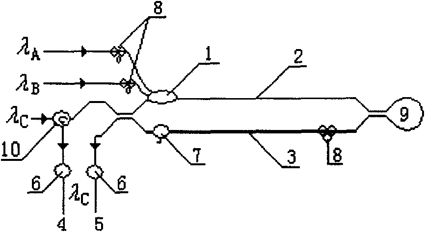
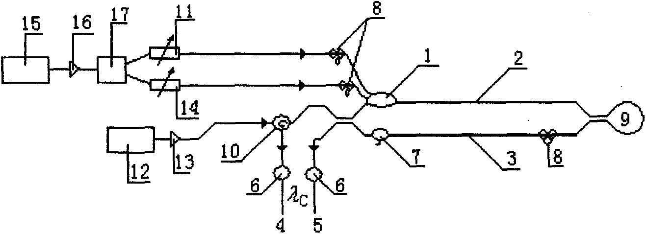
[0048] refer to figure 2 , which shows an experimental model of an all-optical logic gate according to the principles of the present invention. The splitting ratio of the coupler of the Michelson interferometer is 0.5, the arm [2] is a dispersion-shifted fiber, and the nonlinear coefficient γ 1 W -1 km -1 , zero dispersion wavelength λ D , the arm [3] is an ordinary single-mode fiber, and the nonlinear coefficient γ 2 1 W -1 km -1 , the length of both arms is Lkm. The light source [8] is a mode-locked fiber laser, two control lights incident on the Michelson interferometer: wavelength λ A =λ B , pulse width T 1 , peak power P A =P B , the light source [12] is a mode-locked fiber laser, the wavelength λ c , pulse width T 0 , peak power P c . The repetition frequency of the light sources [8] and [12] is the same 10GHz, λ c A D ,T 1 >T 0 , fiber amplifier [9] gain G 1 dB, fiber amplifier [13] gain G 2 dB fiber amplifier [9] gain G 1 dB. Adjustable attenuato...


PUM


Abstract

The invention relates to an all-optical logic gate with a Michelson structure, which can be reused for realizing an AND gate, an OR gate, an NOT gate, an NAND gate, an NOR gate, an XOR gate and an XNOR gate as well as the reverse operation thereof, and also realizing a half-adder. The all-optical logic gate with a Michelson structure comprises two control optical signals, a synchronous optical detection signal and an output detection signal, wherein the two control optical signals are input into an arm (2) of symmetrical Michelson interferometers by a coupler (1); the synchronous optical detection signal is divided into two beams of equal light to be projected into the arm (2) and an arm (3) of the Michelson interferometers and used for outputting a reflecting output opening (4) for expressing the application of the logic result and a transmitting output opening (5) of the reverse operation; the output detection signal is results of the self-phase modulation of a detection optical signal, the intersection phase modulation of the two control optical signals on detection light and average intersection phase modulation on the detection light in two times of arm length and is expressed into a corresponding logic gate relation. The all-optical logic gate has the characteristic of self-phase modulation in the symmetrical Michelson interferometers, preferably the two arms adopt different nonlinear optical fibers and the input arm (2) of the control optical signals adopts a high nonlinear optical fiber.

Description

technical field [0001] The all-optical logic gate of the Michelson structure can be reused to realize the AND gate, the OR gate, the NOT gate, the NAND gate, the NOR gate, the XOR gate, the NOR gate and their inversion operations, and half-addition can also be realized The device belongs to the technical field of optical information processing. Background technique [0002] In the field of optical information processing technology, the ability to perform super-deterministic logic operations on optical signals without converting them back to electrical signals has long been desired. [0003] For example, in order to perform high-speed routing functions in broadband packet-switching networks, the headers of optical data packets require more complex optical signal processing such as synchronization, frame identification, and address identification, and all-optical logic gates are the key components. The all-optical AND gate (AND) can be used to identify the frame header in the...

Claims


Application Information

Patent Timeline
Patent Type & Authority Applications(China)
IPC IPC(8): G02F3/00G02F1/35
Inventor 张利勋刘永智刘永
Owner UNIV OF ELECTRONICS SCI & TECH OF CHINA
Why Eureka
Try Eureka