Electronic component
A technology of electronic components and device chips, applied in the direction of electrical components, electric solid devices, circuits, etc., can solve the problems of low viscosity and difficulty in miniaturization of electronic components, and achieve high air tightness
- Summary
- Abstract
- Description
- Claims
- Application Information
AI Technical Summary
Problems solved by technology
Method used
Image

Examples
Embodiment 1
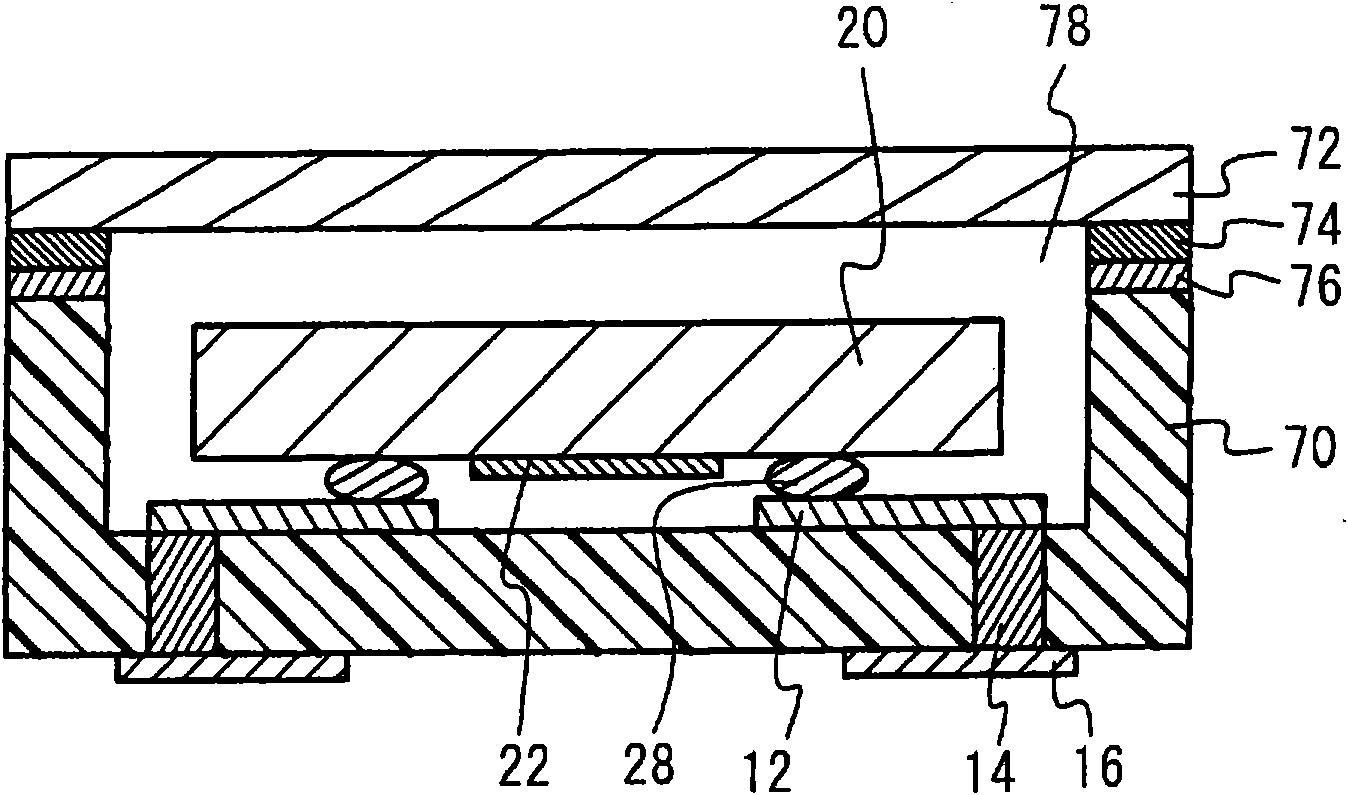
[0044] Figure 5 (a) is a sectional view of the electronic component of Example 1. refer to Figure 5(a), the wiring pattern 12 is provided on the upper surface of the insulating substrate 10 made of ceramics or the like. The lower surface of the insulating substrate 10 is provided with external connection terminals 16 . Internal wiring 14 connecting the wiring pattern 12 and the external connection terminal 16 is provided inside the insulating substrate 10 . A device chip 20 having an active region 22 on a lower surface is mounted on the insulating substrate 10 in a flip-chip manner. That is, the device chip 20 is connected to the wiring pattern 12 via the bump 28 . A pattern 32 is provided on the insulating substrate 10 with a gap between its upper surface and the lower surface of the device chip 20 . SOG oxide film 30 is provided to cover side surfaces of device chip 20 and pattern 32 . And, the SOG oxide film 30 is formed so as to be embedded in the gap between the u...
Embodiment 2
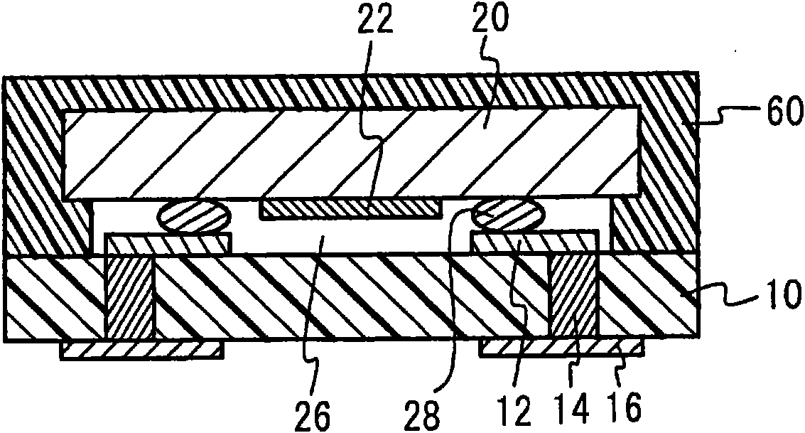
[0054] Embodiment 2 is an example in which a metal film is provided on the outer periphery of the lower surface of the device chip. Figure 9 (a) is a sectional view of the electronic component of Example 2. Figure 9 (b) is a view in which the device chip 20 , the metal film 24 of Cu or Au, and the pattern 32 are seen through from the upper surface of the electronic component of the first embodiment. refer to Figure 9 (a), the metal film 24 is provided on a region of the lower surface of the device chip 20 opposite to the upper surface of the pattern 32 . The lower surface of metal film 24 is covered with SOG oxide film 30 . refer to Figure 9 (b), the metal film 24 is provided in a ring shape along the outer periphery of the device chip 20 . The metal film 24 may not be formed on a part of the outer periphery of the device chip 20 . Other structure and embodiment 1 Figure 5 (a) and Figure 5 (b) is the same, and the explanation is omitted.
[0055] According to Emb...
Embodiment 3
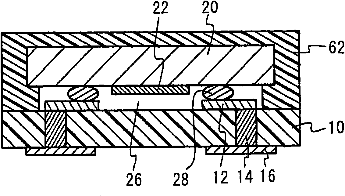
[0057] Embodiment 3 is an example in which driven elements are provided on an insulating substrate. Figure 10 It is a sectional view of the electronic component of Example 3. refer to Figure 10 , a driven element 34 is formed on the insulating substrate 10 opposite to the lower surface of the device chip 20 . The driven element 34 is isolated from the lower surface of the device chip 20 . As the driven element 34 , for example, an inductor formed of metal such as Cu, an MIM (Metal Insulator Metal: Metal Insulator Metal) capacitor formed by laminating a metal film, an insulating film, and a metal film, or the like can be provided. In this way, at least one of capacitance and inductance can be provided as the driven element 34 .
[0058] Electronic components can be miniaturized by forming the driven element 34 between the device chip 20 and the insulating substrate 10 . However, since SOG easily flows into the void 26 because the height of the void 26 is large, it is effe...
PUM
 Abstract
Description
Claims
Application Information