Method and device for large-range and high-resolution atomic force micro detection for large sample

A technology of atomic force microscopy and detection devices, which is applied in the direction of measuring devices, analytical materials, instruments, etc., can solve the problems of detection optical path deviation, inability to realize micro-probe scanning, and separation from micro-probes, etc., and achieve high sensitivity and high resolution , the technical conditions are easy to realize, and the effect of avoiding system errors

Inactive Publication Date: 2009-12-16
ZHEJIANG UNIV
View PDF0 Cites 16 Cited by
  • Summary
  • Abstract
  • Description
  • Claims
  • Application Information

AI Technical Summary

Problems solved by technology

However, conventional AFM probes obviously cannot scan microprobes. For example, when scanning in a large area, the laser and PSD in the detection optical path remain stationary (the reason is that the scanner cannot drive them for fast scanning) , the detection optical path may deviate or even break away from the micro-probe (micro-cantilever) during the scanning process. Therefore, it is necessary to study and design a new AFM probe

Method used


Image

  • Method and device for large-range and high-resolution atomic force micro detection for large sample
  • Method and device for large-range and high-resolution atomic force micro detection for large sample
  • Method and device for large-range and high-resolution atomic force micro detection for large sample

Examples


Embodiment Construction

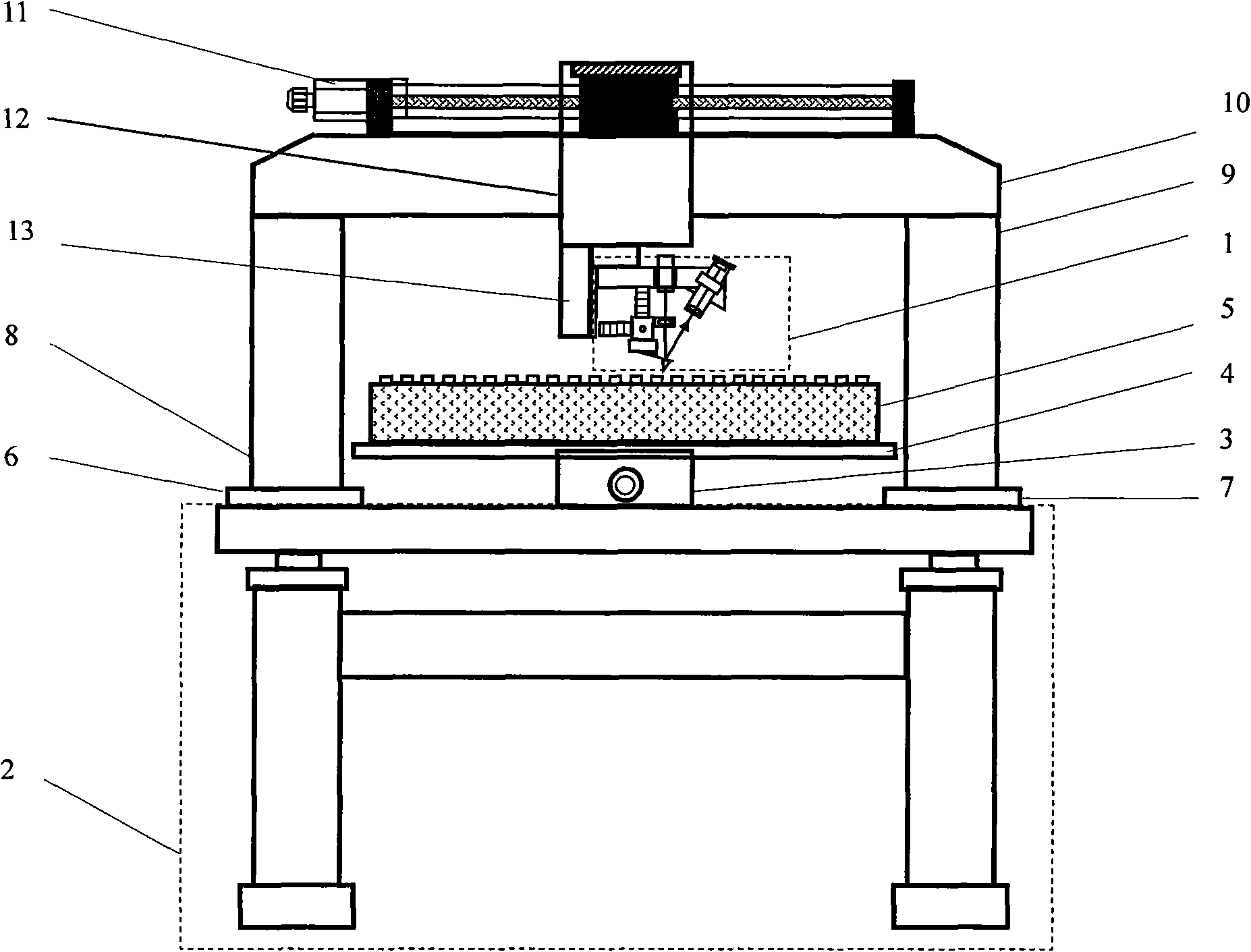
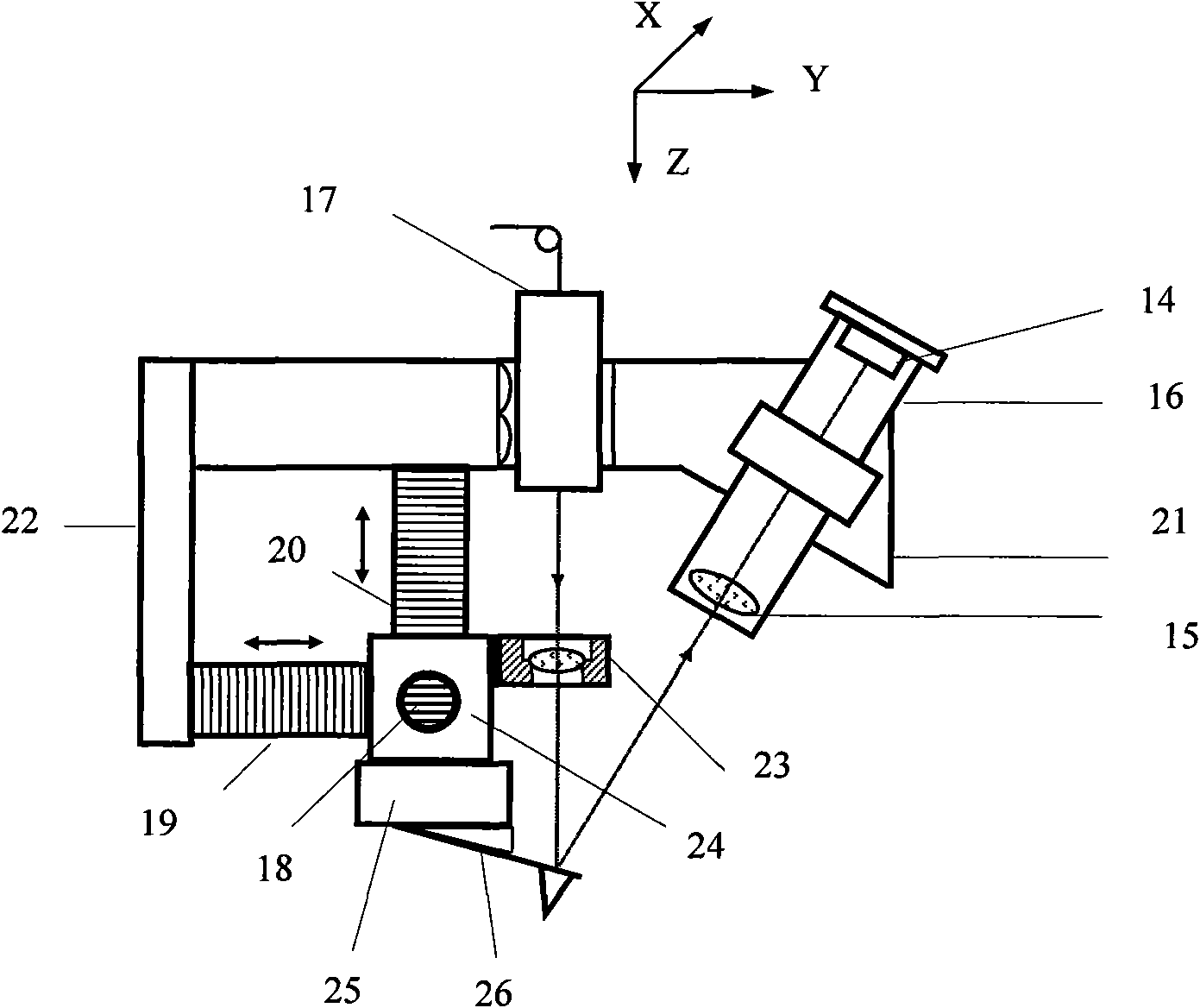
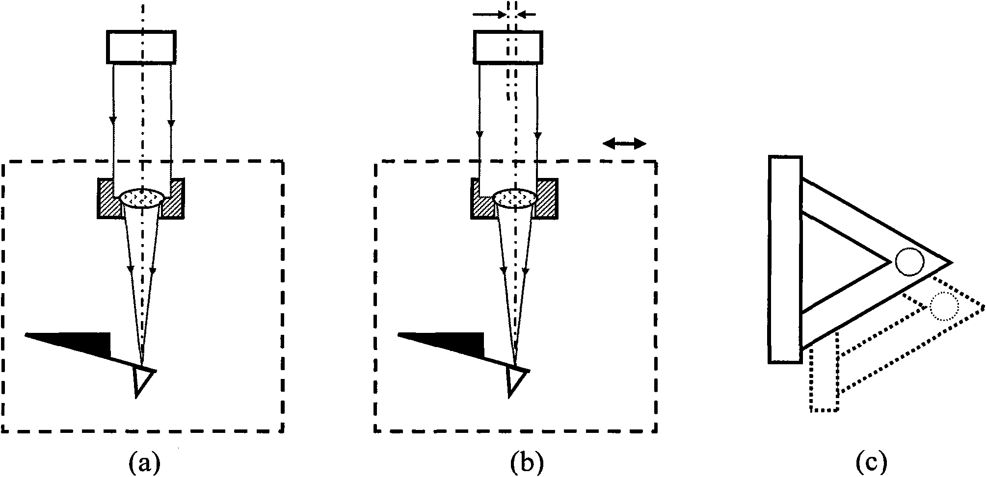
[0017] The method of large-scale high-resolution atomic force microscopy for large samples adopts the method of fixing the sample and scanning the micro-probe, and introduces a small lens that scans together with the scanner. Its XY scanning movement is always the same as that of the micro-probe, that is, the micro-probe The needle is always at the focal point of the small lens. During the wide-range scanning process, the laser spot focused by the small lens is always aligned with the micro-cantilever, thus effectively realizing the tracking of the optical path. Another small spot in front of the photodetector The lens not only avoids the systematic error caused by the Z-direction feedback, but also maintains the high sensitivity and high resolution of the beam deflection method, thereby realizing a large-scale high-precision Z-direction feedback control and a large-scale high-resolution XY scanning imaging ( Horizontal 0.2nm, vertical 0.1nm), using an open sample stage and a t...


PUM


Abstract

The invention discloses a method and a device for large-range and high-resolution atomic force micro detection for a large sample. By adopting a method combining the scanning of a piezoelectric ceramic probe and the large-range motion of a step motor and designing an open sample stage, the micro-nano detection of large-sized super-precise workpieces is realized. The device is provided with a large-range and high-resolution scanning probe system, an X-Y-axis step electric translation stage, an optical platform and a scan imaging and feedback control system, wherein the large-range and high-resolution scanning probe system consists of a laser, a light path tracking lens, piezoelectric ceramics, a micro cantilever probe and a photoelectric detection element; and the X-Y-axis step electric translation stage is used for moving large-sized samples in large range. The method and the device have the advantages of overcoming the limitation that a conventional AFM is only suitable for small-range detection of small samples, designing a simple and practical lens system to solve the light path tracking problem when the probe scans in the large range, and adopting the open sample stage and the two-dimensional step motor to realize large-range scanning and detection in any area for the large-sized super-precise workpiece samples under the condition of keeping the ultra-high resolution of the AFM.

Description

technical field [0001] The invention relates to a large-scale, large-scale, high-resolution atomic force microscopic detection method and device. It is used for micro-nano inspection of large samples such as ultra-precision workpieces, large optical components, large lenses, large aperture diffractive optical devices, and large gratings. Background technique [0002] Micro-nano technology is a frontier subject field that has developed rapidly in the world in recent years, and the micro-nano detection technology mainly represented by scanning probe microscope (SPM) technologies such as atomic force microscope (AFM) and scanning tunneling microscope (STM) is a micro-nano detection technology. An important basis and prerequisite for technological development. In particular, AFM has a larger application field because it is not limited by the conductivity of the sample. At present, the vast majority of AFMs in the world, or conventional AFMs, use microprobes to fix the probes a...

Claims


Application Information

Patent Timeline
Patent Type & Authority Applications(China)
IPC IPC(8): G01N13/16
CPCG01Q10/02G01Q20/02G01Q10/04
Inventor 张冬仙谢志刚章海军
Owner ZHEJIANG UNIV
Why Eureka
Try Eureka