Image sensor and column processing circuit thereof

A column processing and circuit technology, which is applied in the field of column processing circuits and image sensors, can solve problems such as easy distortion of light intensity signals

Active Publication Date: 2009-12-16
BRIGATES MICROELECTRONICS KUNSHAN
View PDF0 Cites 13 Cited by
  • Summary
  • Abstract
  • Description
  • Claims
  • Application Information

AI Technical Summary

Problems solved by technology

[0006] During the test, it was found that the light intensity voltage signal output by the prior art column processing circuit is prone to distortion relative to the light intensity signal exposed on the pixel array

Method used


Image

  • Image sensor and column processing circuit thereof
  • Image sensor and column processing circuit thereof
  • Image sensor and column processing circuit thereof

Examples


Embodiment 1

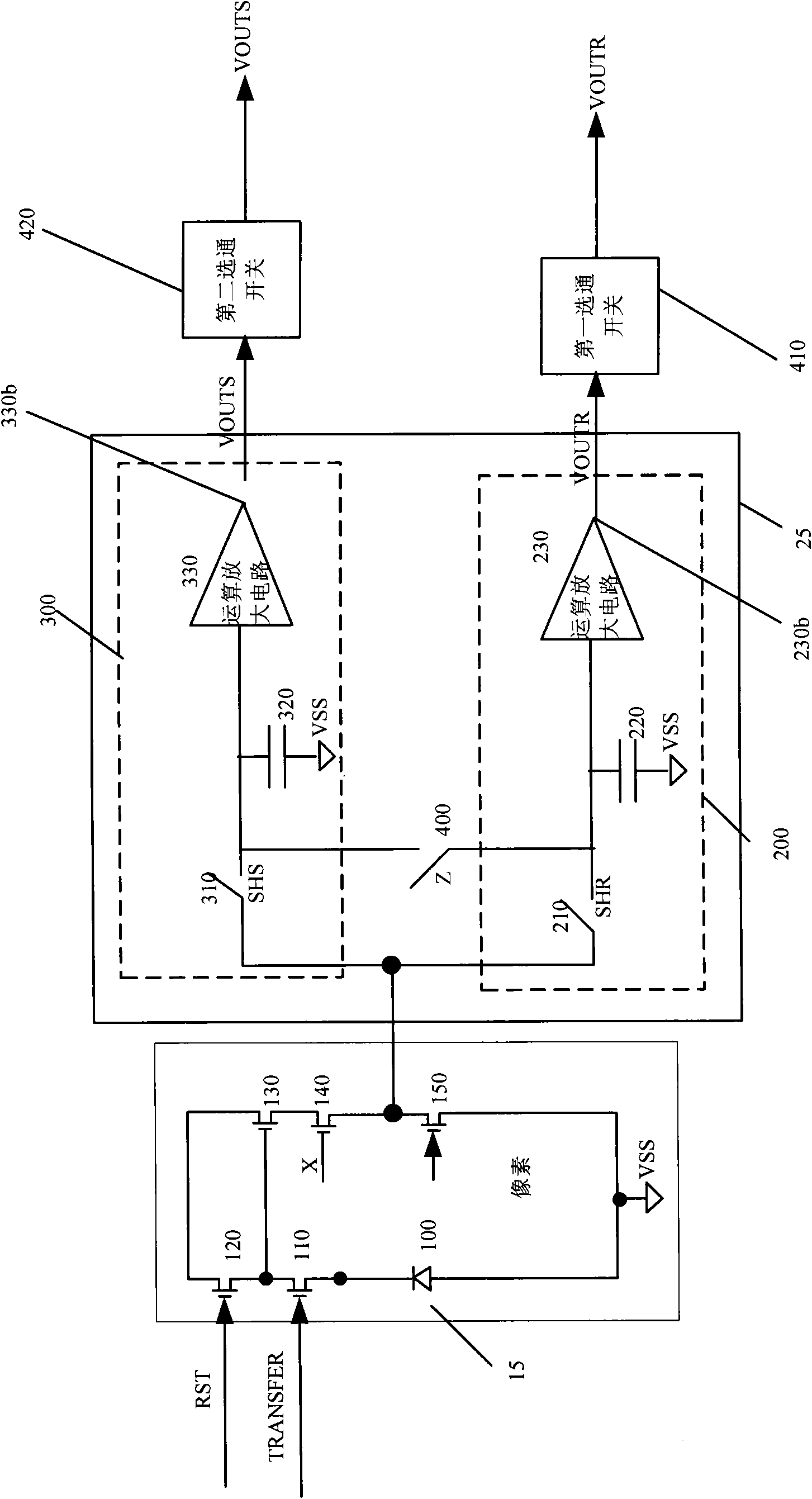
[0039] image 3 Shown is a schematic structural diagram of a pixel and a column processing unit in the image sensor according to the first embodiment of the present invention.

[0040] Such as image 3 As shown, the pixel 15 includes: a photodiode 100 , a first NMOS transistor 110 , a second NMOS transistor 120 , a third NMOS transistor 130 , a fourth NMOS transistor 140 and a bias NMOS transistor 150 .

[0041] Wherein, the anode of the photosensitive diode 100 is connected to the low level VSS, the negative electrode of the photosensitive diode 100 is connected to the source of the first NMOS transistor 110; the gate of the first NMOS transistor 110 is connected to the transmission signal input terminal (TRANSFER), and the first NMOS transistor 110 The drain of the second NMOS transistor 120 is connected to the source of the second NMOS transistor 120; the drain of the second NMOS transistor 120 is connected to the high level VDD, and the gate of the second NMOS transistor ...

no. 2 example

[0067] Figure 9 Shown is a schematic diagram of a second embodiment of the column processing circuit of the present invention. In this embodiment, the same parts as those in the first embodiment will not be repeated. The difference is that in this embodiment, a second-stage operational amplifier circuit 430 is also included, and the input terminals of the second-stage operational amplifier circuit 430 are connected to at least two The output of the operational amplifier circuit 230 of the reference voltage unit 200 , for example, can be connected to 2 operational amplifier circuits 230 , to 3 operational amplifier circuits 230 , to 6 operational amplifier circuits 230 and so on. Such as Figure 9 As shown, the input terminal of the second-stage operational amplifier circuit 430 is connected to the outputs of the operational amplifier circuits 230 of the two reference voltage units 200 . The output end of the second-stage operational amplifier circuit 430 is connected to the...

no. 3 example

[0071] Figure 10 Shown is a schematic diagram of a third embodiment of the column processing circuit of the present invention. In this embodiment, the same parts as those in the first embodiment will not be described again. The difference is that in this embodiment, the column processing unit 25 also includes a third-stage operational amplifier circuit 440, and the first stage of at least two reference voltage units 200 The output end of the two-stage operational amplifier circuit 430 is connected to the input end of the third-stage operational amplifier circuit 440, and the output end of the third-stage operational amplifier circuit 440 is connected to the first selection switch 410, wherein the third-stage operational amplifier circuit 440 is Connected as an operational amplifier circuit in the form of a voltage follower. For example, it may have the same structure as the second-stage operational amplifier circuit 430 connected thereto. Similarly, the light intensity volt...


PUM


Abstract

The invention provides an image sensor and a column processing circuit thereof. A column processing unit of the column processing circuit comprises a reference voltage unit, an optical intensity voltage unit and a differential output switch, wherein the reference voltage unit comprises a control switch and an operational amplifier circuit which are sequentially connected in series from an input end to an output end as well as a grounding capacitor with one end being connected between the control switch and a voltage follower; the optical intensity voltage unit comprises a control switch and an operational amplifier circuit which are sequentially connected in series from an input end to an output end as well as a grounding capacitor with one end being connected between the control switch and a voltage follower; one end of the differential output switch is connected between the control switch of the optical intensity voltage unit and the operational amplifier circuit of the reference voltage unit, and the other end is connected between the control switch of the optical intensity voltage unit and the operational amplifier circuit of the optical intensity voltage unit, wherein the operational amplifier circuit is connected in a way of the voltage follower. The invention improves the precision of an optical intensity voltage signal output by the column processing circuit.

Description

technical field [0001] The invention relates to the technical field of image information, in particular to a column processing circuit of an image sensor and the image sensor. Background technique [0002] Such as figure 1 As shown, an existing image sensor includes a pixel array 10, a column processing circuit 20 connected to the pixel array 10, an analog-to-digital converter 30 connected to the column processing circuit 20, and a digital processing circuit connected to the analog-to-digital converter 30 40. [0003] The pixel array 10 is composed of several pixels (photosensitive units) 15, and the pixels 15 can perceive the light intensity of a dot area. Since the pixel array 10 has a plurality of pixels 15 arranged in rows and columns, and subsequent circuits cannot process such a large amount of data at the same time, the column processing circuit 20 has a plurality of column processing units 25 and multiplex switches (not shown), Each column processing unit 25 is re...

Claims


Application Information

Patent Timeline
Patent Type & Authority Applications(China)
IPC IPC(8): H04N3/15H04N5/335H04N5/3745
Inventor 罗文哲陈巨韩明
Owner BRIGATES MICROELECTRONICS KUNSHAN
Why Eureka
Try Eureka