Micro electromechanical system piezoelectric transducer and manufacturing method thereof

A technology of piezoelectric transducers and micro-electromechanical systems, applied in the manufacture/assembly of piezoelectric/electrostrictive devices, piezoelectric/electrostrictive/magnetostrictive devices, circuits, etc., can solve the problem of transducer static Capacitance cannot be effectively reduced, weakening the effectiveness of the series connection of array elements, and the inability to directly realize the electrical series connection of array elements, etc.

Active Publication Date: 2019-01-18
徐景辉
View PDF21 Cites 16 Cited by
  • Summary
  • Abstract
  • Description
  • Claims
  • Application Information

AI Technical Summary

Problems solved by technology

However, for the current transducers based on piezoelectric ceramics, due to the limitation of the manufacturing process, the electrical series connection between the array elements cannot be directly realized during the manufacturing process, and must be realized through the back-end circuit connection, but the back-end circuit connection is usually ...

Method used


Image

  • Micro electromechanical system piezoelectric transducer and manufacturing method thereof
  • Micro electromechanical system piezoelectric transducer and manufacturing method thereof
  • Micro electromechanical system piezoelectric transducer and manufacturing method thereof

Examples


Embodiment 1

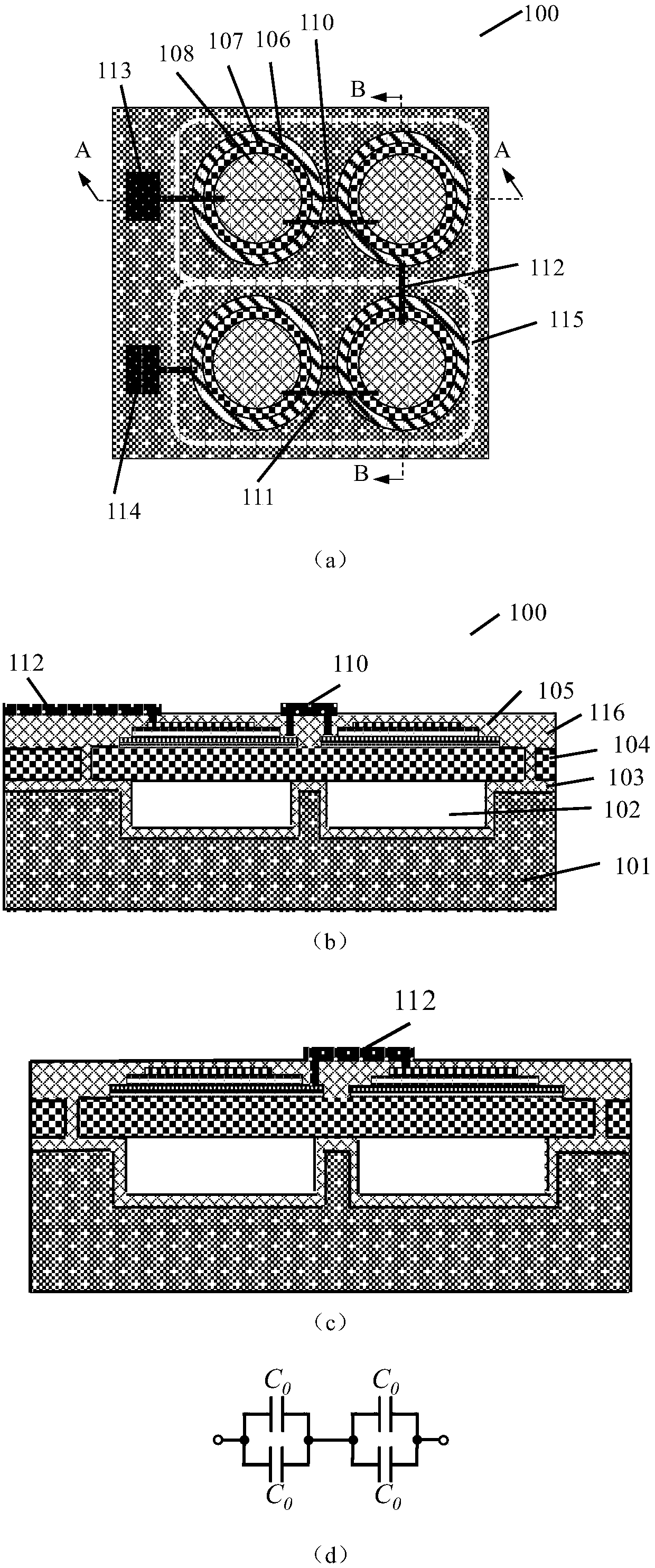
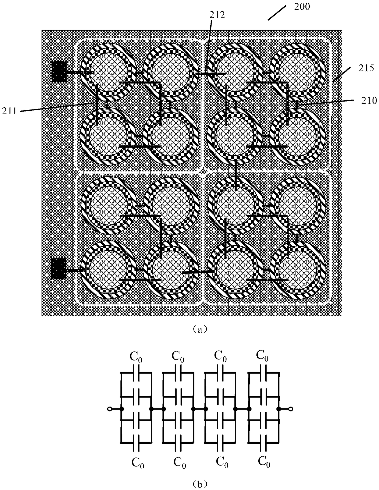
[0066] This embodiment serves as a top view of a typical array MEMS piezoelectric transducer as figure 1 as shown in (a), figure 1 (b) is along figure 1 Sectional view of line A-A of (a); figure 1 (c) is along figure 1 (a) Cross-sectional view of line B-B. like figure 1 As shown in (a), the piezoelectric transducer 100 in this embodiment is composed of four piezoelectric array elements. like figure 1As shown in (b), the transducer consists of a substrate 101 including four cavities 102, a buried oxide layer 103 and a device layer 104 on the substrate 101, a piezoelectric stack 105 on the device layer 104, and an insulating layer 116 located on the piezoelectric stack 105 . The buried oxide layer 103 and the device layer 104 together constitute the supporting layer of the transducer; the piezoelectric stack 105 is composed of a piezoelectric seed layer 106 , a lower electrode 107 , a piezoelectric functional layer 108 and an upper electrode 109 . The four array elements...

Embodiment 2

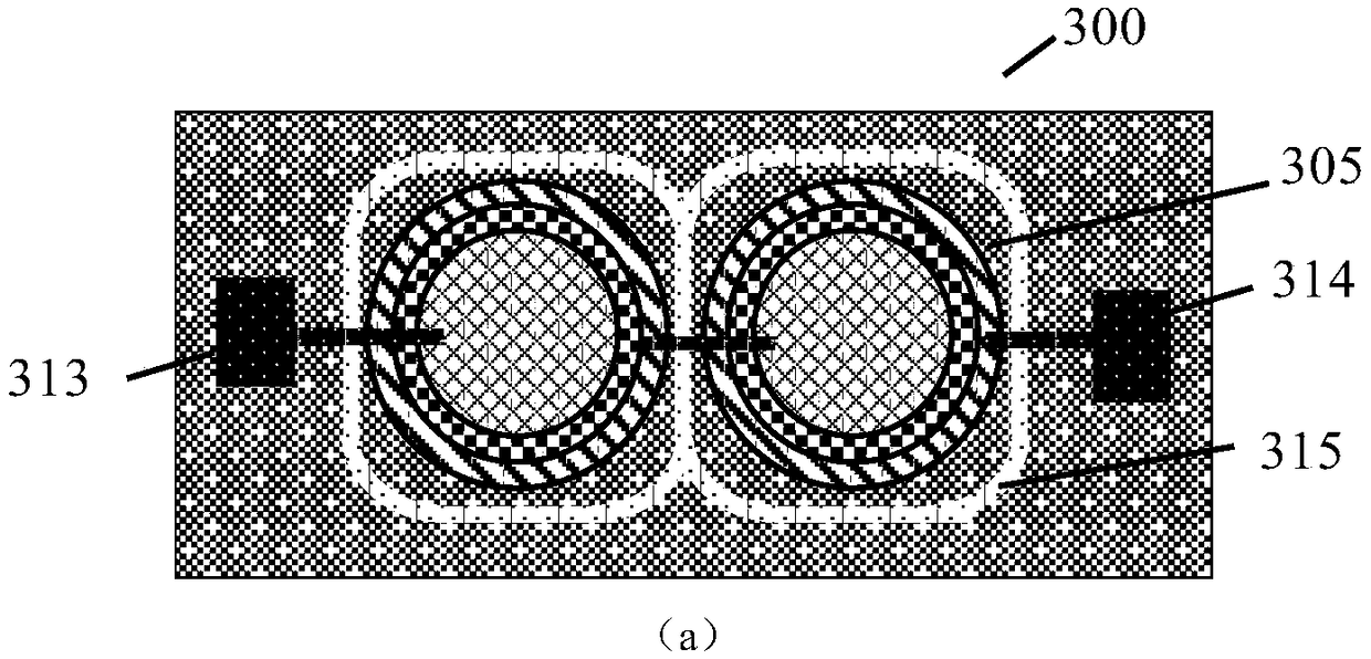
[0075] image 3 (a) is another example proposed by the present invention, two piezoelectric array elements form a row, and an electrical series is formed between the array elements, image 3 (b) for image 3 (a) Sectional view. refer to image 3 , the piezoelectric transducer 300 is composed of two piezoelectric array elements, and the transducer consists of a substrate 301 containing two cavities 302, a buried oxide layer 303 and a device layer 304 located on the substrate 301, located in the device Piezoelectric stack 305 on top of piezoelectric stack 304 , insulating layer 316 on top of piezoelectric stack 305 , and solderable electrode layers 317 , 318 on top of insulating layer 316 . Among them, the buried oxide layer 303 and the device layer 304 together constitute the supporting layer of the transducer; the piezoelectric stack 305 is a double piezoelectric stack, which consists of the piezoelectric seed layer 306, the lower electrode 107, and the first piezoelectric ...

Embodiment 3

[0082] Figure 4 The present invention proposes a piezoelectric array transducer with two array elements connected in series and a manufacturing method thereof.

[0083] 1) Reference Figure 4 (a), (b), the process starts from the common wafer substrate 401, and adopts deep reaction ion etching (DRIE) or reaction ion etching (RIE) method according to the design of the transducer A plurality of cavities 402 are formed by etching on the surface of the wafer; and then a layer of oxide 403 is evenly deposited.

[0084] 2) Reference Figure 4 (c), (d), introduce a piece of SOI (Silicon on insulator) wafer 500 , which is composed of substrate layer 501 , buried oxide layer 503 and device layer 504 . Combine SOI wafer 500 with Figure 4 (b) The wafers with the cavity 402 and the oxide layer 403 are bonded face to face at high temperature to form a bonded new wafer 600 .

[0085] 3) Reference Figure 4 (e) The substrate layer 501 and the buried oxide layer 503 of the wafer 600 a...


PUM

PropertyMeasurementUnit
Thicknessaaaaaaaaaa

Abstract

The invention discloses a micro-electromechanical system piezoelectric transducer and a manufacturing method thereof, in particular an array piezoelectric transducer and a manufacturing method, and belongs to the micro-electromechanical system field. The transducer adopts array design and is composed of at least two array elements. The wafer-level electrical series connection or parallel connection between the array elements is realized by a micro-electromechanical system (MEMS) process compatible with the semiconductor process, but at least one electrical series connection is provided; Semiconductor MEMS process can effectively control the parasitic capacitance generated by electrical series and parallel connection, thus effectively improve the sensitivity. The invention improves the sensitivity of the transducer through the wafer-level electric series and parallel connection between the array elements. Compared with the traditional piezoelectric ceramic transducer, the parasitic capacitance caused by the following circuit string and parallel connection is avoided. A wafer-level array MEMS transducer is proposed. The array transducer can be connected in series with different arrayelements according to the needs, so that the sensitivity of the transducer can be defined independently. The transducer also has the advantages of high signal-to-noise ratio, low cost, low electricalnoise and high signal-to-noise ratio.

Description

Technical field: [0001] The invention relates to a microelectromechanical system piezoelectric transducer and a manufacturing method thereof, in particular to an array piezoelectric transducer and a manufacturing method, belonging to the field of microelectromechanical systems. Background technique: [0002] Piezoelectric effect: When some dielectrics are deformed by external forces in a certain direction, polarization will occur inside them, and at the same time, opposite charges will appear on its two opposite surfaces. When the external force is removed, it will return to an uncharged state; when the direction of the force changes, the polarity of the charge also changes. This phenomenon is called the positive piezoelectric effect. On the contrary, when an electric field is applied in the polarization direction of the dielectric, these dielectrics will also deform. After the electric field is removed, the deformation of the dielectric will disappear. This phenomenon is ca...

Claims


Application Information

Patent Timeline
IPC IPC(8): H01L41/113H01L41/27H01L41/332
CPCH10N30/30H10N30/05H10N30/082Y02P70/50
Inventor 徐景辉
Owner 徐景辉
Why Eureka
Try Eureka