Solid-state imaging device, drive method thereof and electronic apparatus

A solid-state imaging device and charge technology, which is applied in semiconductor devices, radiation control devices, televisions, etc., can solve problems such as afterimages and difficult charge transmission, and achieve the effects of increased sensitivity and increased saturation charge

Active Publication Date: 2009-12-23
SONY CORP
View PDF7 Cites 62 Cited by
  • Summary
  • Abstract
  • Description
  • Claims
  • Application Information

AI Technical Summary

Problems solved by technology

[0041] However, in the invention utilizing the light absorption characteristics in the wavelength and depth directions as in Patent Document 1, it is necessary to form a photoelectric sensor for photoelectric conversion of red light having a longer wavelength at a depth of about 2 μm from the surface of the Si substrate 3100 . diode
Therefore, the distance from the output terminal on the surface of the Si substrate 3100 is long, so it is extremely difficult to completely transfer the charges accumulated in the photodiode, which may cause afterimages

Method used


Image

  • Solid-state imaging device, drive method thereof and electronic apparatus
  • Solid-state imaging device, drive method thereof and electronic apparatus
  • Solid-state imaging device, drive method thereof and electronic apparatus

Examples


Embodiment 1

[0198] Example including two vertical gate electrodes

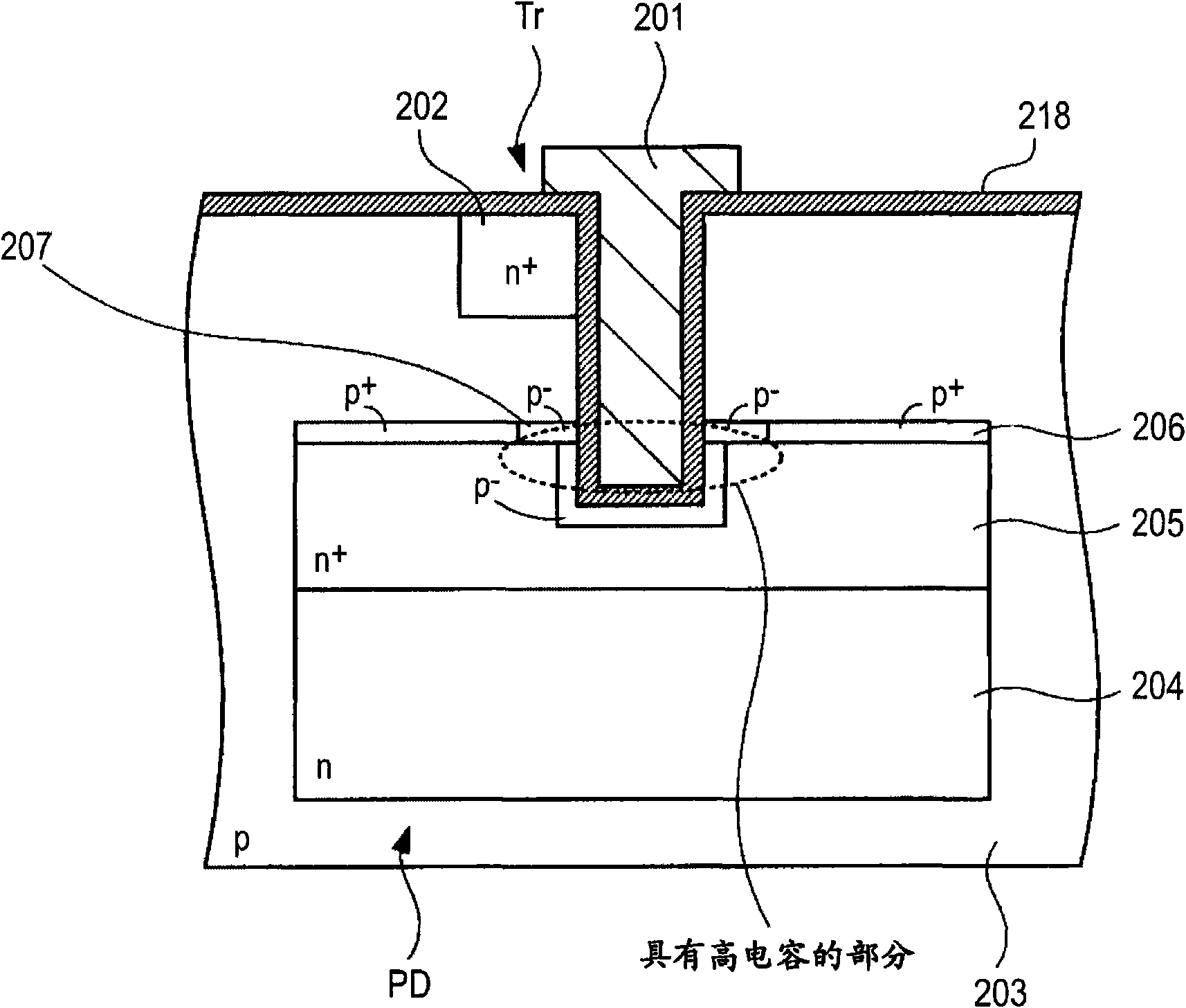
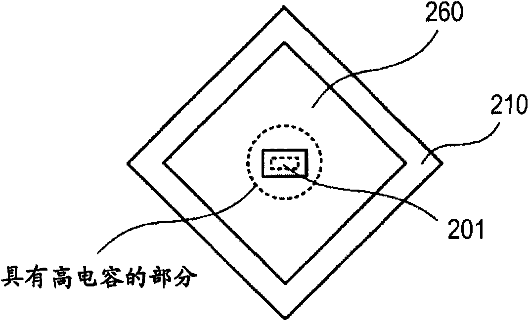
[0199] Image 6 A schematic planar structure of a solid-state imaging device according to Embodiment 1 of the present invention is shown, Figure 7 shows along the Image 6 Schematic cross-sectional structure of line A-A in . Image 6 with Figure 7 are top and cross-sectional views of the relevant parts contained in a pixel. Such as Image 6 with Figure 7 As shown, the solid-state imaging device includes a photodiode PD and a charge readout transistor Tr formed in a semiconductor substrate 13 . The charge readout transistor Tr includes two vertical gate electrodes 12 a , 12 b formed at the peripheral portion of the photodiode PD and a floating diffusion region 11 formed at the corner of the photodiode region 60 near the outer region. In this embodiment, a case where the first conductivity type is the p type and the second conductivity type is the n type will be described.

[0200] The semiconductor substrate 13 ...

Embodiment 2

[0218] Example including two vertical gate electrodes

[0219] Figure 9 A schematic planar structure of a solid-state imaging device according to Embodiment 2 of the present invention is shown, Figure 10 A cross-sectional structure along line B-B is shown. This embodiment differs from Embodiment 1 in the formation position of the floating diffusion region 11 . exist Figure 9 with Figure 10 in, with Image 6 with Figure 7 Corresponding parts are denoted by the same reference numerals, and repeated explanations are omitted.

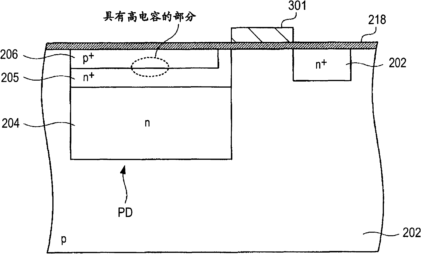
[0220] In the solid-state imaging device of this embodiment, the floating diffusion region 11 is formed on the surface side of the semiconductor substrate 13 from the corner of the photodiode region 60 sandwiched by the vertical gate electrodes 12a, 12b to the inside of the photodiode region 60 . The floating diffusion region 11 is shared between the two vertical gate electrodes 12a, 12b. In the present embodiment, the floating diffusion region...

Embodiment 3

[0224] Example including two vertical gate electrodes and horizontal gate electrodes

[0225] Figure 11 A schematic planar structure of a solid-state imaging device according to Embodiment 3 of the present invention is shown, Figure 12 shows along the Figure 11 The cross-sectional structure of the C-C line in . exist Figure 11 with Figure 12 in, with Image 6 with Figure 7 Corresponding parts are denoted by the same reference numerals, and repeated explanations are omitted.

[0226] In the solid-state imaging device of the present embodiment, the charge readout transistor Tr included in one pixel includes a horizontal gate electrode 19 , vertical gate electrodes 12 a and 12 b , and a floating diffusion region 11 .

[0227] Two vertical gate electrodes 12 a , 12 b are formed at the outer peripheral portion of the photodiode region 60 , respectively, along both edges constituting the corners of the photodiode region 60 . On the upper surface of the semiconductor su...


PUM


Abstract

The invention discloses a solid-state imaging device, a drive method thereof and an electronic apparatus using the same. A solid-state imaging device includes: plural photodiodes formed in different depths in a unit pixel area of a substrate; and plural vertical transistors formed in the depth direction from one face side of the substrate so that gate portions for reading signal charges obtained by photoelectric conversion in the plural photodiodes are formed in depths corresponding to the respective photodiodes. The electronic apparatus using the solid-state imaging device has increased saturated charge quantity (Qs), improved sensitivity and reduced pixel size. The drive method of the solid-state imaging device can reduce the pseudo color, image retention, noise and color mixture and improve the sensitivity.

Description

[0001] Cross References to Related Applications [0002] This application contains information related to the prior Japanese patent applications JP2008-150963, JP 2008- 285907, JP 2008-285908 and JP 2008-285909, the entire contents of which are hereby incorporated by reference. technical field [0003] The present invention relates to a solid-state imaging device having a plurality of photodiodes in a unit pixel area thereof, a driving method of the solid-state imaging device, and an electronic device using the solid-state imaging device. Background technique [0004] Color separation in a CCD image sensor or a CMOS image sensor, which is a solid-state imaging device, is mainly realized by using a color filter. In an image sensor using a color filter, one color filter is mounted for one pixel, and generally three pixel circuits having red, green, and blue filters are arranged adjacent to each other. Therefore, in a narrow sense, the light available in one pixel is only one...

Claims


Application Information

Patent Timeline
Patent Type & Authority Applications(China)
IPC IPC(8): H01L27/146H01L29/78H01L29/06H01L31/08H04N5/335H01L31/10H04N5/357H04N5/369H04N5/374
Inventor 渡部泰一郎山田明大城户英男西藤洋将马渕圭司大岸裕子
Owner SONY CORP
Why Eureka
Try Eureka