Portable electric power communication protocol detector and detection method thereof
A power communication and portable technology, which is applied in the direction of electrical components, circuit devices, digital transmission systems, etc., can solve problems such as failure to find messages, unknown structure, difficult analysis, etc., to avoid further expansion and solve lost messages , the effect of a complete and effective analysis
- Summary
- Abstract
- Description
- Claims
- Application Information
AI Technical Summary
Problems solved by technology
Method used
Image

Examples
Embodiment 1
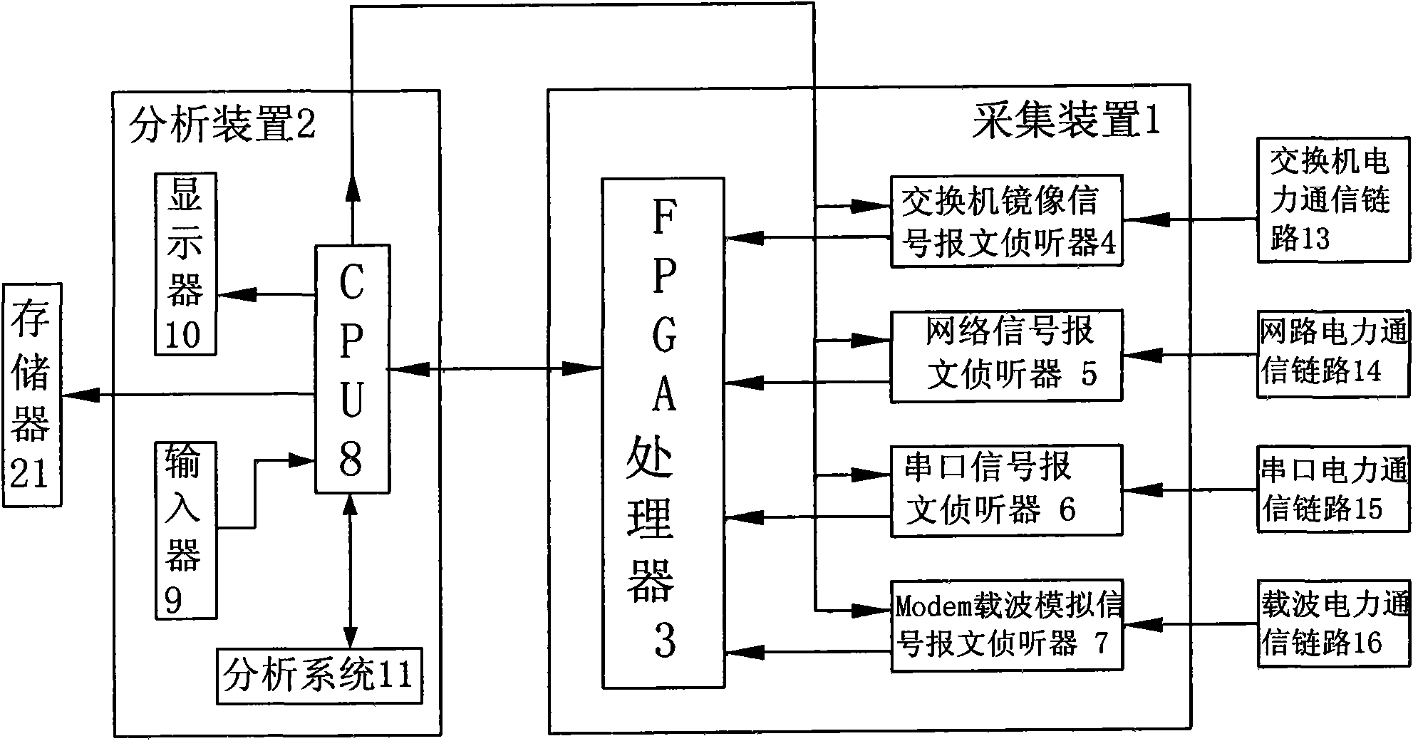
[0058] The portable power communication protocol detector of this embodiment is as figure 1 with figure 2 As shown, it includes an acquisition device 1 and an analysis device 2 arranged in a hand-held case. Acquisition device 1 contains message listener and parallel-to-serial processor; Listener 6 and MODEM carrier signal message listener 7 are composed of four message listeners, and the parallel-to-serial processor is composed of FPGA processor 3. Analysis device contains CPU8, analysis system 11, input device 9 and display 10 connected with CPU8 respectively; Wherein, CPU8 adopts embedded processor (model is MPC8377), input device 9 adopts keyboard, mouse or touch screen input device etc., display 10 adopt general CRT or liquid crystal display. The respective input terminals of the above four message listeners are respectively connected to the exchange communication link 13, the network communication link 14, the serial port power communication link 15 and the carrier po...
Embodiment 2
[0087] The portable power communication protocol detector of this embodiment is basically the same as that of Embodiment 1, the difference is that the FPGA processor 3 is replaced by a plurality of single-chip microcomputers working together.
[0088] The detection method of the present embodiment is slightly different from the first embodiment, and the difference except the same steps is:
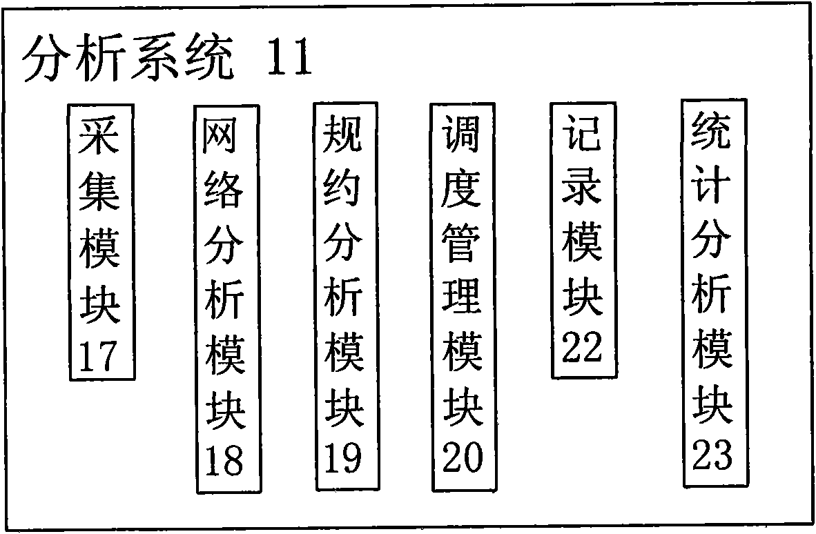
[0089] 1. The specific association designation in step 1) is to select the protocol analysis module 19 corresponding to the specific protocol of the power communication link to be detected;
[0090] 2. The protocol analysis module 19 in step 2 is a non-universal module that forms the grammatical and semantic environment of a specific statute through program design and performs grammatical and semantic analysis on a specific statute, that is, there are multiple statute analysis modules inside the analysis system, different The specifications of are identified by different specification anal...
PUM
 Abstract
Description
Claims
Application Information
 - R&D
- Intellectual Property
- Life Sciences
- Materials
- Tech Scout
- Unparalleled Data Quality
- Higher Quality Content
- 60% Fewer Hallucinations
Browse by: Latest US Patents, China's latest patents, Technical Efficacy Thesaurus, Application Domain, Technology Topic, Popular Technical Reports.
© 2025 PatSnap. All rights reserved.Legal|Privacy policy|Modern Slavery Act Transparency Statement|Sitemap|About US| Contact US: help@patsnap.com