Realization method for improving chip yield

A realization method and a technology of yield rate, applied in the field of structural design and implementation to improve chip yield, can solve problems such as cost loss, increase design, verification, and test cycles, and achieve the effects of improving yield rate, balanced configuration, and high technical value

Active Publication Date: 2010-01-20
LANGCHAO ELECTRONIC INFORMATION IND CO LTD
View PDF0 Cites 16 Cited by
  • Summary
  • Abstract
  • Description
  • Claims
  • Application Information

AI Technical Summary

Problems solved by technology

Multiple chip castings not only increase the cycle of design, verification, and testing, but also the expensive chip production costs also cause cost losses in the entire chip R&D and production process

Method used


Image

  • Realization method for improving chip yield
  • Realization method for improving chip yield
  • Realization method for improving chip yield

Examples


Embodiment

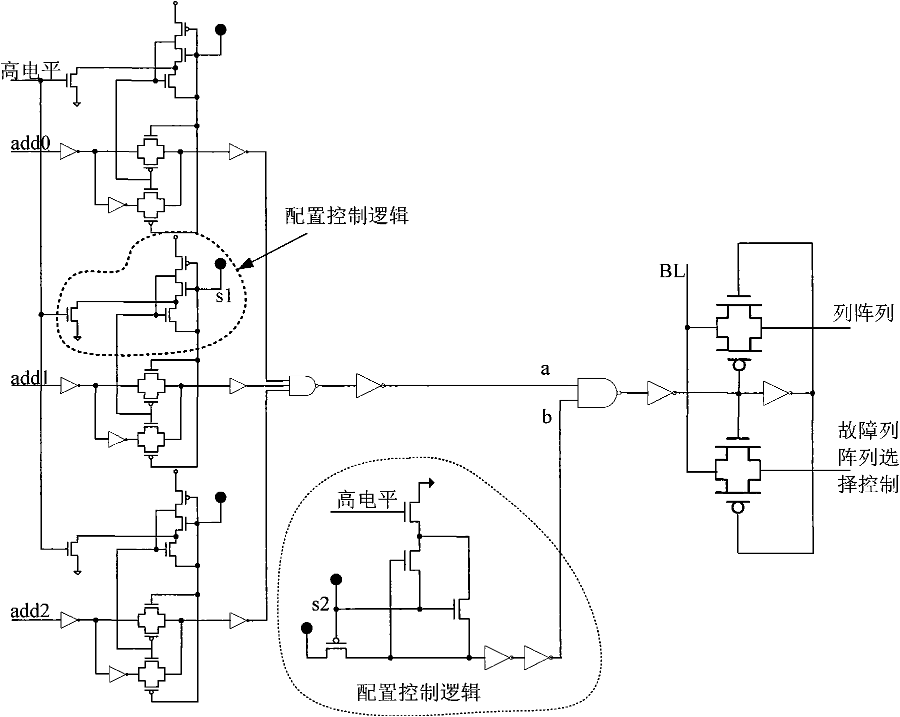
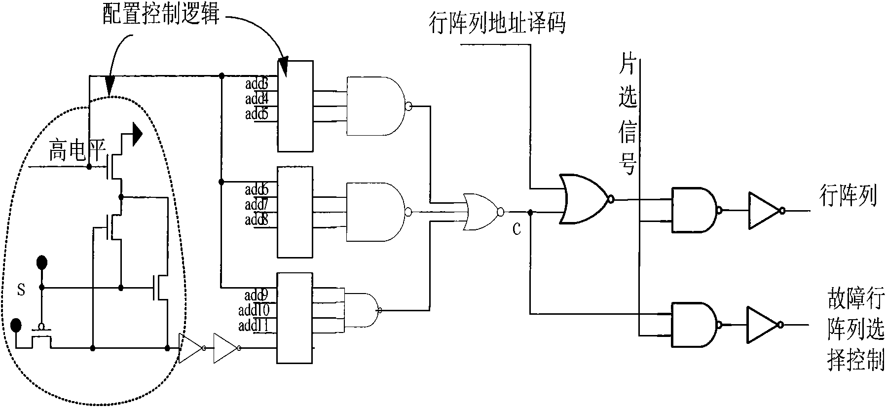
[0016] The method for repairing the defects of the storage array in the present invention mainly includes: a storage array column unit fault repairing method, a storage array row unit repairing method, a fuse control efficient implementation method, and a redundant array dynamic expansion method.

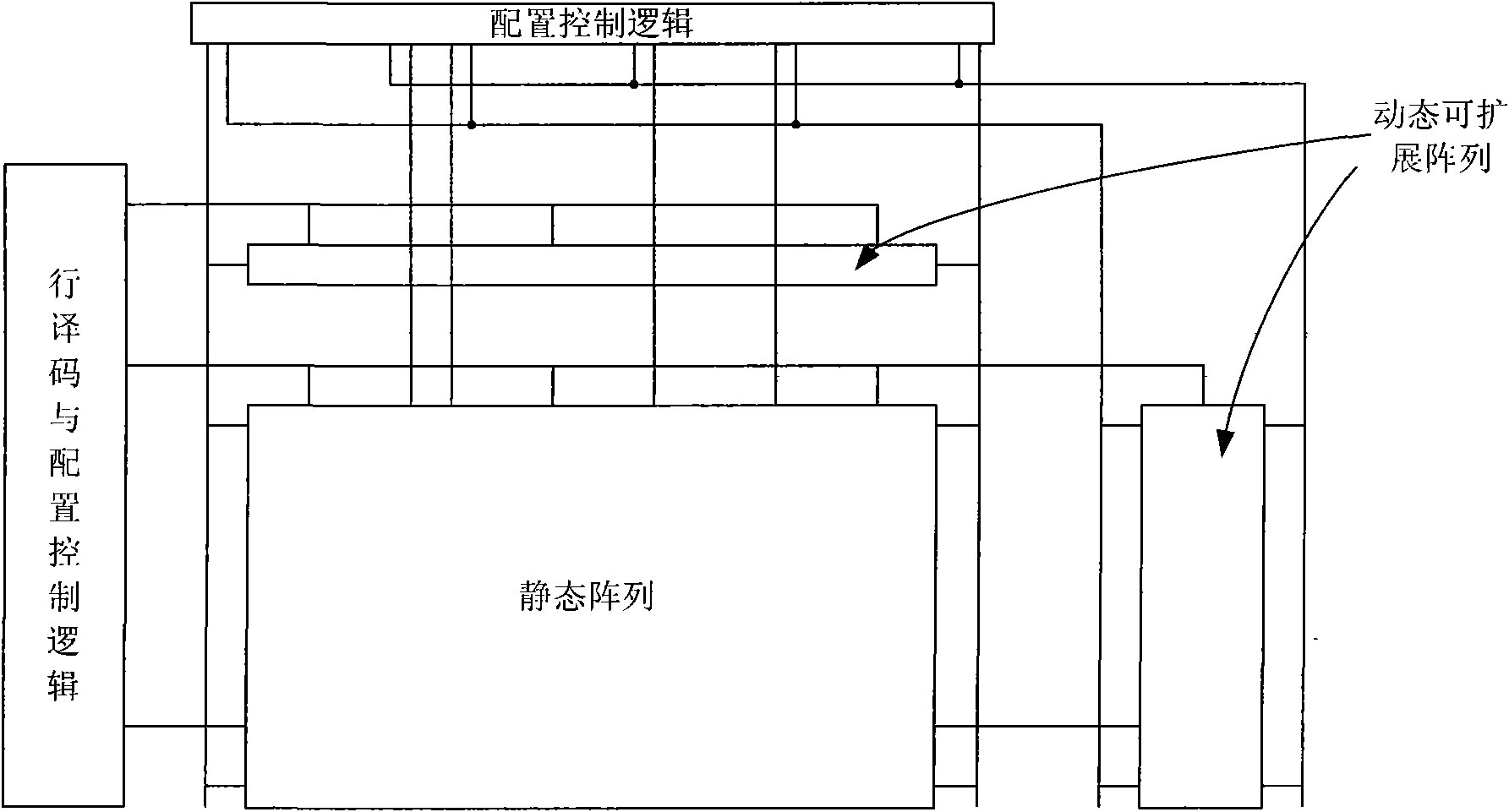
[0017] The redundant structure of the dynamic memory array in this paper includes: a dynamic redundant column array and a dynamic redundant row array, which are respectively located above and to the right of the static memory array, which is considered for the decoding logic and the layout of the layout. Redundant array configuration control logic modules are also divided into row array configuration logic and column array configuration logic. The configuration control selection signal adopts top-level wiring, which makes it very easy for the laser programming method to control whether to select redundant column arrays or row arrays. easy to accomplish.

[0018] The steps of redunda...


PUM


Abstract

The invention provides a design method for improving chip yield. In the method, chip yield is improved by adopting the methods of dynamic memory array redundant structure configuration, array defect reparation and power-on protection circuit. The design of the dynamic memory array redundant structure configuration comprises an on-ship memory array logical structure design, an on-ship memory array territory structure design, a top layer fuse control logic module and a protection circuit design; a defective column unit is replaced by designing a redundant column array, and a defective row unit is replaced by designing a redundant row array in the dynamic memory array; when a certain column with faults and defects is discovered in the testing process for the storage parts, the top layer fuse control logic module and the protection circuit are connected with a standby redundant column array or redundant row array by programming a fuse unit connected with a column decoder so as to replace the corresponding part with faults and defects so that fault reparation of the whole chip and improvement of chip yield are realized.

Description

technical field [0001] The invention relates to the field of integrated circuit design, in particular to a structural design implementation method for improving chip yield. Background technique [0002] With the rapid development of integrated circuit technology, in order to meet people's needs, large-capacity storage capacity has increasingly become a basic feature of high-performance microprocessors, which requires embedding large-capacity memories inside the chip. It is possible to build more powerful chips to better accommodate the greater demand for memory in today's various chip applications, but on the other hand, it is also caught in the dilemma of larger chip sizes and lower yields. Because the increase of the internal memory ratio of the chip is the main reason for the failure of the chip, the process deviation caused by the higher and higher integration density is one of the main reasons for the decrease of the chip yield. The increase in the number of memories o...

Claims


Application Information

Patent Timeline
Patent Type & Authority Applications(China)
IPC IPC(8): G06F17/50
Inventor 李仁刚
Owner LANGCHAO ELECTRONIC INFORMATION IND CO LTD
Why Eureka
Try Eureka