
Semiconductor memory device

A storage device and semiconductor technology, applied in the direction of information storage, static memory, digital memory information, etc., can solve the problems of voltage drop, high power consumption, and inability to provide a large enough storage unit, so as to achieve improved reliability, low power consumption, The effect of reducing power consumption

Inactive Publication Date: 2010-02-03
PANASONIC CORP
View PDF1 Cites 0 Cited by
  • Summary
  • Abstract
  • Description
  • Claims
  • Application Information

AI Technical Summary

Problems solved by technology

However, if the current capability is lowered, a voltage drop occurs, and there is a problem that a sufficient drain voltage cannot be supplied to the drain of the memory cell.
In addition, since the conventional drain voltage generating circuit is configured to discharge the voltage supplied from the gate of the transistor to the ground node except when writing data, there is a problem of large power consumption.

Method used


Image

  • Semiconductor memory device
  • Semiconductor memory device
  • Semiconductor memory device

Examples


Embodiment Construction

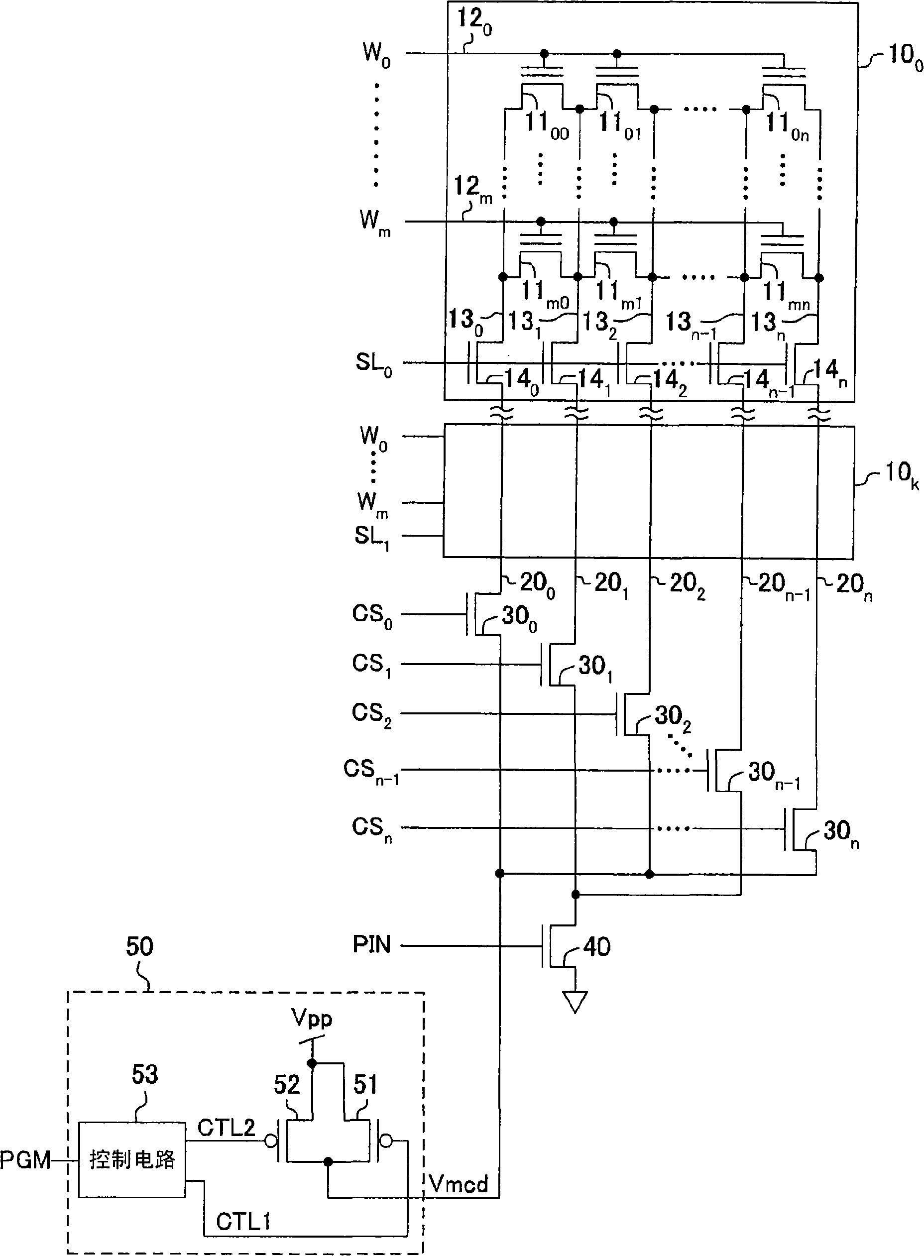
[0022] figure 1 It shows the structure of the semiconductor memory device which concerns on one Embodiment of this invention. The semiconductor storage device of this embodiment is provided with k+1 sub-arrays 10 0 ~10 k A subarray semiconductor memory device. Subarray 10 0 ~10 k Each has (m+1)×(n+1) memory cells 11 arranged in a matrix 00 ~11 mn . And, corresponding to storage unit 11 00 ~11 mn Each row of is provided with m+1 word lines 12 0 ~12 m . That is, each word line 12 is connected to the gates of n+1 memory cells 11 belonging to the same row. In addition, corresponding to the storage unit 11 00 ~11 mn Each column is provided with n+1 bit lines 13 0 ~13 n . That is, the even-numbered bit line 13 is connected to the drains of (m+1)×2 memory cells 11 belonging to adjacent columns, and the odd-numbered bit line 13 is connected to (m+1)×2 memory cells 11 belonging to adjacent columns. Source connection of memory cell 11.

[0023] Additionally, the subar...


PUM


Abstract

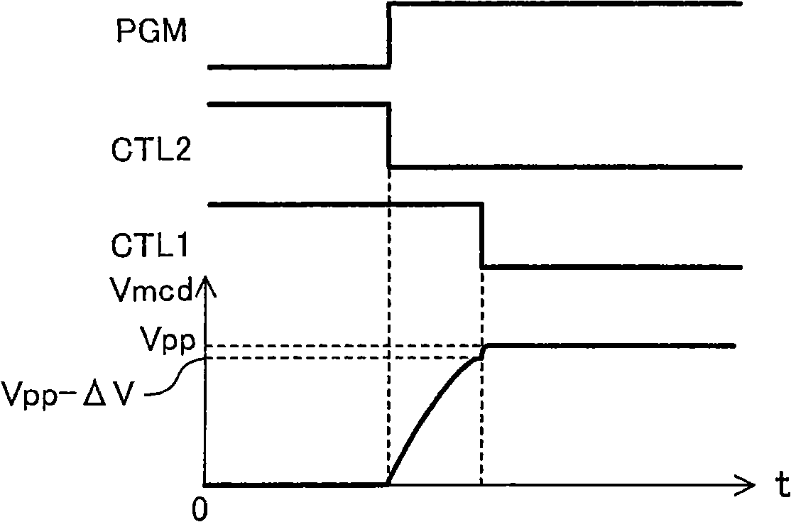
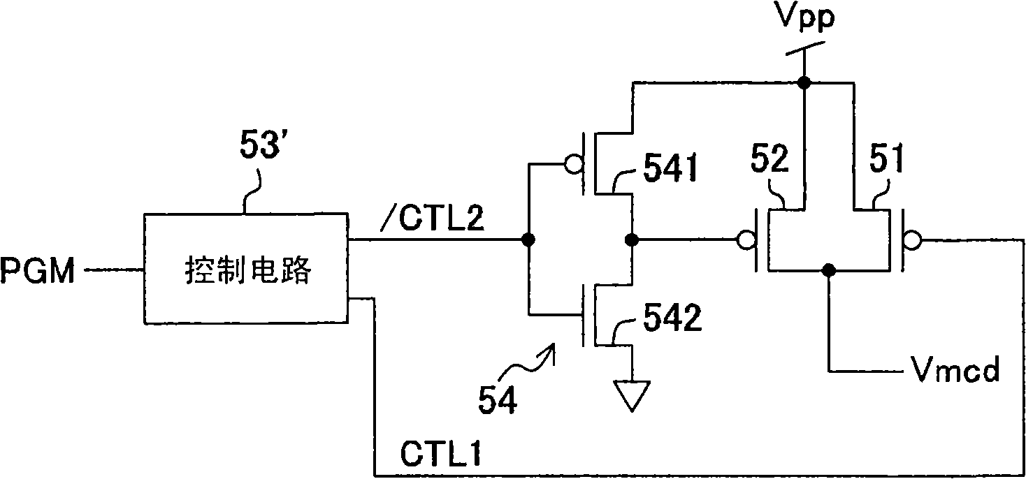
The invention provides a semiconductor memory device which can fully ensure the rising time of the drain voltage of a memory cell in such as EEPROM, has low power consumption and supplies high enoughvoltage to the memory cell. A drain voltage generator circuit (50) includes a first switching element (51) coupled between a first power supply voltage and an output end of the drain voltage generatorcircuit, a second switching element (52) coupled in parallel to the first switching element (51) and having a smaller current capability than that of the first switching element (51), and a control circuit (53) for turning ON the second switching element (52) and then the first switching element (51), and generates a voltage to supply to a drain of a memory cell (11). A source of the memory cell(11) is set to be floated or grounded by a transistor (40).

Description

technical field [0001] The present invention relates to a semiconductor memory device, in particular to a non-volatile memory such as EEPROM (Electrically Erasable Programmable Read Only Memory). Background technique [0002] In EEPROM, the storage content of the storage unit can be deleted and rewritten through electrical signals. Specifically, the word line connected to the gate of the memory cell is activated to select the memory cell, a prescribed voltage is applied to the drain of the memory cell according to a control signal for writing data into the memory cell, and the source is changed to a ground state or Floating state. When the source of the memory cell is grounded, thermal electrons are injected into the memory cell, and L data is written as a result. On the other hand, if the source of the memory cell is in a floating state, a tunnel current is generated, and as a result, H data is written. [0003] When the drain voltage of a memory cell is rapidly raised, ...

Claims


Application Information

Patent Timeline
IPC IPC(8): G11C7/12H03K5/13
Inventor 持田礼司富田泰弘河野和幸春山星秀中山雅义
Owner PANASONIC CORP
Learn More