Electronic device, thin-film transistor, display device and conductor contact process

A technology for thin film transistors and electronic devices is applied in the field of conductor contact technology and electronic devices with a multi-layer metal structure, which can solve the problems of high cost of the multi-layer metal structure, and achieve low material cost, high production yield, and improved electrical properties. quality effect

Inactive Publication Date: 2010-02-10
INNOLUX CORP
View PDF0 Cites 7 Cited by
  • Summary
  • Abstract
  • Description
  • Claims
  • Application Information

AI Technical Summary

Problems solved by technology

[0005] The present invention provides an electronic device to solve the problem of high cost of multilayer metal structures in known electronic devices

Method used


Image

  • Electronic device, thin-film transistor, display device and conductor contact process
  • Electronic device, thin-film transistor, display device and conductor contact process
  • Electronic device, thin-film transistor, display device and conductor contact process

Examples


Embodiment Construction

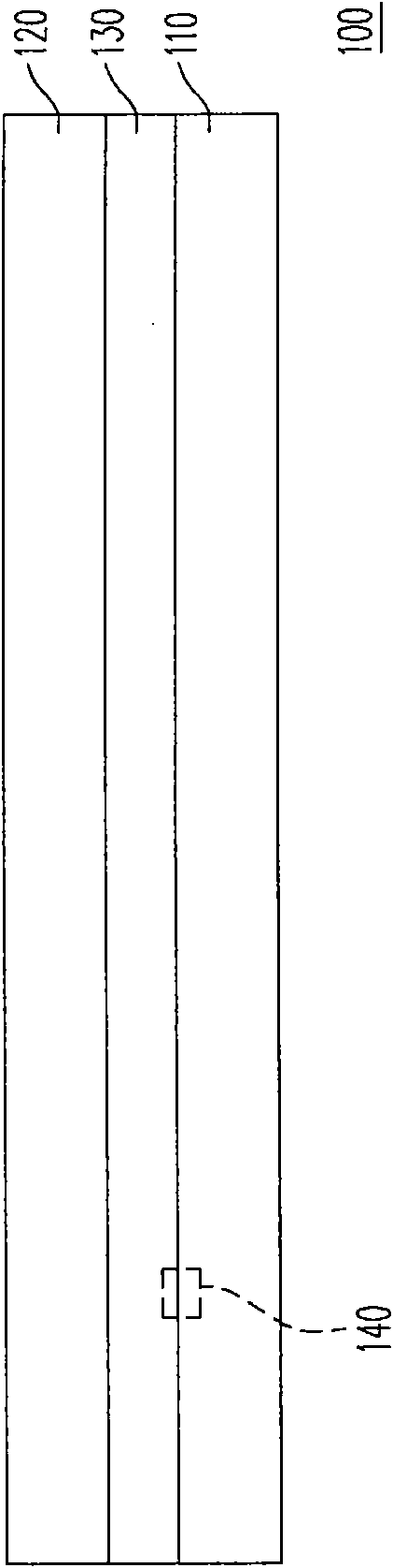
[0059] figure 1 Shown is a display device according to an embodiment of the present invention. Please refer to figure 1 , the display device 100 includes a first substrate 110 , a second substrate 120 and a display medium 130 located between the first substrate 110 and the second substrate 120 . For example, when the display device 100 is a liquid crystal display device, the first substrate 110 is, for example, an active element array substrate, the second substrate 120 is, for example, a color filter, and the display medium 130 is, for example, a liquid crystal layer. Of course, the display device 100 may also be a plasma display device, an organic electroluminescence display device or other types of display devices. When the display device 100 is an organic electroluminescence display device, it may also only have a first substrate 110 and an organic light emitting layer disposed on the first substrate 110 as the display medium 130 . In this embodiment, the first substrat...


PUM


Abstract

The invention relates to an electronic device, a thin-film transistor, a display device and conductor contact process. The electronic device is at least provided with a conductor pattern configured ona substrate. The conductor pattern comprises a substantive pure aluminum layer and an aluminum nickel lanthanide alloy layer, the substantive pure aluminum layer is configured on the substrate, and the aluminum nickel lanthanide alloy layer is configured on the substantive pure aluminum layer. The electronic device has the advantages of low manufacturing cost, good electrical property and good manufacturing yield.

Description

technical field [0001] The present invention relates to an electronic device, a thin film transistor, a display device and a conductor contact process, and in particular to an electronic device with a multilayer metal structure, a thin film transistor, a display device and a conductor contact process. Background technique [0002] In the general semiconductor process or the metallization process of liquid crystal displays, aluminum (Al), molybdenum (Mo), tantalum (Ta), chromium (Cr), tungsten (W) and other metals or their alloys are generally used as the metal layer. materials, among which aluminum is the most commonly used. Aluminum is the most abundant metal on the earth. It is cheap and has many characteristics, such as low resistivity, good adhesion to the substrate, and good etching characteristics. Taking the common switching element thin film transistor as an example, aluminum is often used as the material of the gate and source / drain metal layers. [0003] However,...

Claims


Application Information

Patent Timeline
Patent Type & Authority Applications(China)
IPC IPC(8): H01L29/49H01L29/43H01L29/786H01L23/532
Inventor 王程麒林志展石世民
Owner INNOLUX CORP
Why Eureka
Try Eureka