
Method for chemical mechanical polishing

A chemical-mechanical, grinding-layer technology, applied in electrical components, semiconductor/solid-state device manufacturing, circuits, etc., can solve problems affecting device performance, excessive grinding, etc., to avoid device performance, avoid excessive grinding, and achieve selective grinding. Effect

Active Publication Date: 2012-03-07
SEMICON MFG INT (SHANGHAI) CORP
View PDF2 Cites 0 Cited by
  • Summary
  • Abstract
  • Description
  • Claims
  • Application Information

AI Technical Summary

Problems solved by technology

[0005] The invention provides a method of chemical mechanical grinding, which solves the problem of extremely excessive grinding that may occur in the existing technology, thereby affecting the performance of the device

Method used


Image

  • Method for chemical mechanical polishing
  • Method for chemical mechanical polishing
  • Method for chemical mechanical polishing

Examples


Embodiment approach

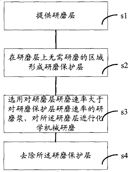
[0013] refer to figure 1 Shown, a kind of embodiment of the method for chemical mechanical polishing of the present invention comprises:

[0014] Step s1, providing a grinding layer;

[0015] Step s2, forming a grinding protective layer on the grinding layer on the area that does not need grinding;

[0016] Step s3, selecting a slurry whose grinding rate for the grinding layer is greater than the grinding rate for the grinding protective layer, and performing chemical mechanical grinding on the grinding layer;

[0017] Step s4, removing the grinding protection layer.

[0018] In a specific embodiment, the grinding layer can be the excess polysilicon layer that needs to be removed during the process of forming the erasing gate and the device gate in the memory process, or it can be the local thickness adjustment or surface smoothing that needs to be performed in other processes Adjusted material layers.

[0019] However, before chemical mechanical polishing, the grinding pr...


PUM

PropertyMeasurementUnit
thicknessaaaaaaaaaa

Abstract

The invention relates to a method for chemical mechanical polishing, which comprises the following steps: forming a polishing protective layer in an area without needing to be polished on a polishing layer; and selecting a polishing paddle which has a higher polishing speed on the polishing layer than the polishing speed on the polishing protective layer to perform chemical mechanical polishing of the polishing layer. The method for the chemical mechanical polishing avoids the over-polishing on the area without needing to be polished, thereby preventing a polishing process from influencing the device performance.

Description

technical field [0001] The invention relates to the field of semiconductor manufacturing, in particular to a chemical mechanical grinding method. Background technique [0002] With the development of semiconductor manufacturing technology, the size of the memory is gradually reduced, however, the voltage for programming and erasing the memory is not reduced to the same extent. Therefore, reducing the programming and erasing voltage becomes one of the main challenges for the further scaling of flash memory. [0003] At present, a common solution is to use an additional erasing gate in the storage unit of the memory, and reduce the erasing voltage by increasing the coupling with the floating gate. For example, Chinese patent application No. 200580019839.9 discloses a nonvolatile memory device, comprising: a substrate with a substrate surface; at least two isolation regions in the substrate surface, the isolation regions have a floating gate extending over the substrate betwe...

Claims


Application Information

Patent Timeline
Patent Type & Authority Patents(China)
IPC IPC(8): H01L21/304
Inventor 蒋莉邵颖黎铭琦
Owner SEMICON MFG INT (SHANGHAI) CORP
Learn More