

Light-emitting device, electronic equipment, and process of producing light-emitting device
A technology for light-emitting devices and light-emitting elements, which can be used in identification devices, semiconductor/solid-state device manufacturing, circuits, etc., and can solve problems such as Ag atom condensation.
- Summary
- Abstract
- Description
- Claims
- Application Information
AI Technical Summary
Problems solved by technology
Method used
Image

Examples
no. 2 Embodiment approach
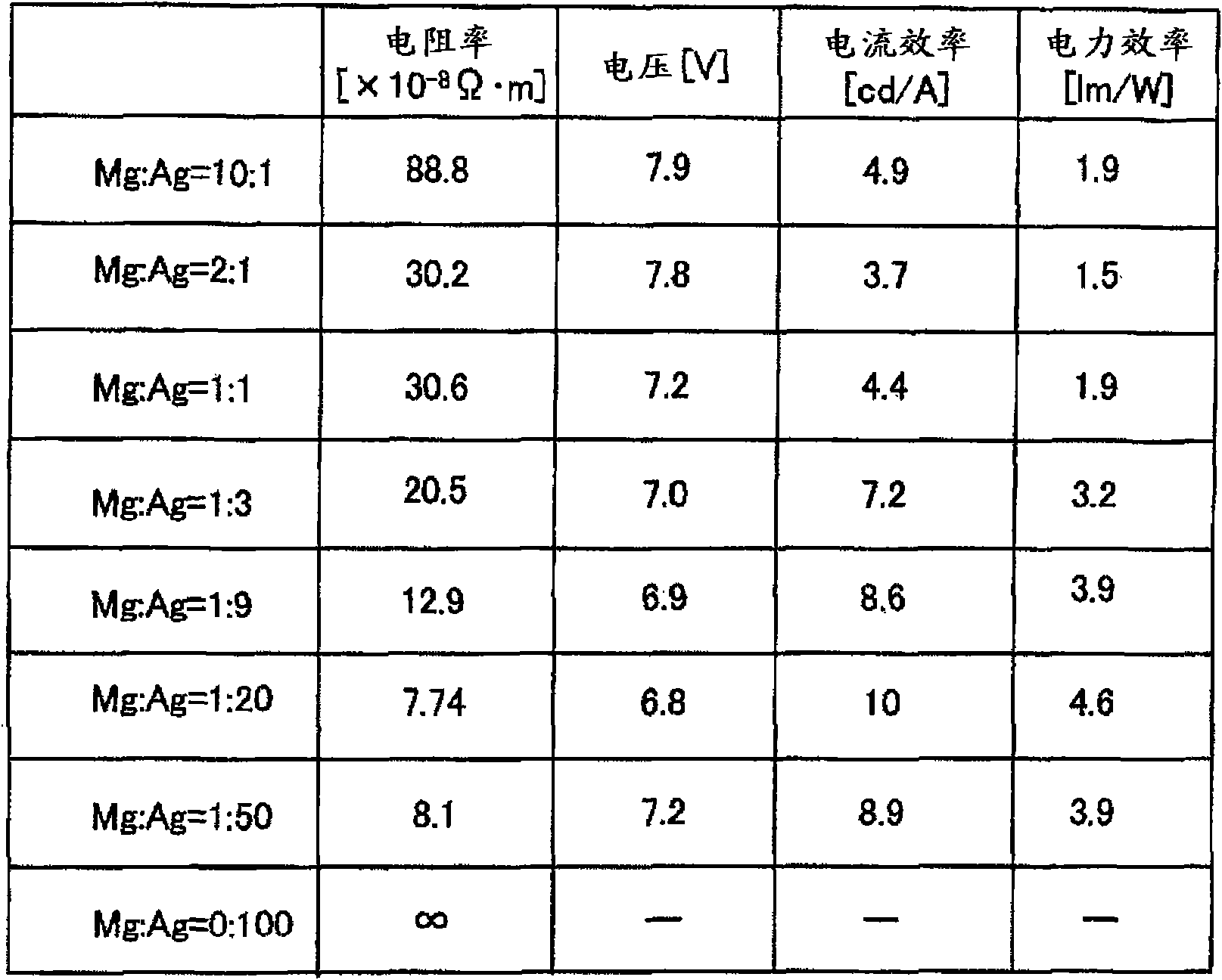
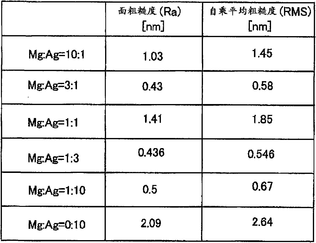
[0121] In the second embodiment, the vapor deposition rate ratio of Mg and Ag forming the counter electrode 20 is set to 1:9. Since other configurations are the same as those of the above-mentioned first embodiment, descriptions of overlapping parts are omitted.
[0122] Figure 11 It is a graph showing measurement results of various data when the film thickness of the counter electrode 20 in the light-emitting element Ug of the second embodiment is 10 nm, 13 nm, and 16 nm, respectively. Figure 11 The shown sheet resistance represents the sheet resistance of the counter electrode 20, Figure 11 The data of the voltage, current efficiency, and power efficiency shown here assume that the density of the current flowing through the counter electrode 20 is 17.5 mA / cm 2 time data. In addition, although illustration is omitted, the values of various data when the film thickness of the counter electrode 20 is 20 nm are equivalent to the values of various data when the film thi...
example 2
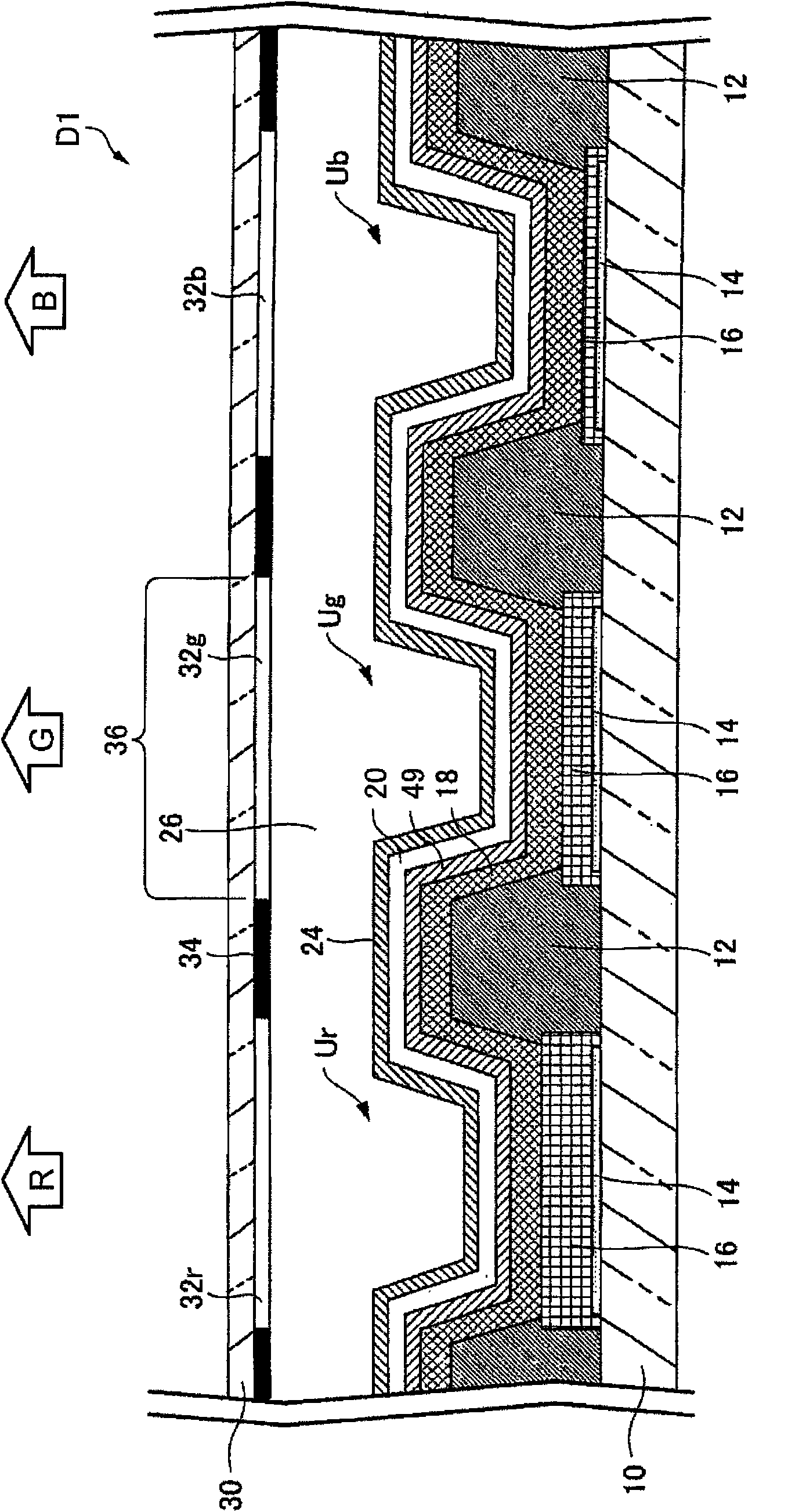
[0247] In the light-emitting devices ( D1 to D10 ) according to the above-described embodiments, in order to improve the purity (color purity) of emitted light, the color filter 32 is provided on the light emitting side. However, it is not limited to this form, and for example, a form in which no color filter 32 is provided may also be employed.
[0248] like Figure 12 The light-emitting device D2 of the third embodiment shown, or Figure 22 Like the light-emitting device D4 of the fifth embodiment shown, by forming the light-emitting functional layer 18 for each light-emitting color of the light-emitting element U, it is possible to use three types of light-emitting elements (Ur, Ug, Ub) without using the color filter 32. Emit high-purity light.
[0249] Figure 34 This is a light-emitting device of a modified example having a configuration similar to that of the light-emitting device D9 according to the tenth embodiment, and the light-emitting functional layer 18 is formed...
Deformed example 3
[0251] In each of the above-mentioned embodiments, the opposite electrode 20 is the cathode of the light emitting element U, but may also be an anode.
[0252] (4) Modification 4
[0253] In the light-emitting device D9 according to the tenth embodiment, the region on the counter electrode 20 that overlaps with the central portion of the region of the light-emitting element U partitioned by the partition wall 12 is not covered with the stress relaxation layer 22 . However, the present invention is not limited thereto, and, for example, an embodiment may be adopted in which the entire region overlapping with the region of the light-emitting element U in the region on the counter electrode 20 is not covered by the stress relaxation layer 22 .
[0254] In addition, in the light-emitting device D9 according to the tenth embodiment, the region overlapping the partition wall 12 on the counter electrode 20 is completely covered with the stress relaxation layer 22, but it is not limit...
PUM
| Property | Measurement | Unit |
|---|---|---|
| Resistivity | aaaaa | aaaaa |
| Film thickness | aaaaa | aaaaa |
| Film thickness | aaaaa | aaaaa |
Abstract
Description
Claims
Application Information