CMOS circuits with high-k gate dielectric

A dielectric and gate technology, applied in the field of CMOS structure, can solve problems such as structure and technology that have not yet been proposed

Inactive Publication Date: 2010-03-03
IBM CORP
View PDF0 Cites 5 Cited by
  • Summary
  • Abstract
  • Description
  • Claims
  • Application Information

AI Technical Summary

Problems solved by technology

So far, no such structure and technology have been proposed

Method used


Image

  • CMOS circuits with high-k gate dielectric
  • CMOS circuits with high-k gate dielectric
  • CMOS circuits with high-k gate dielectric

Examples


Embodiment Construction

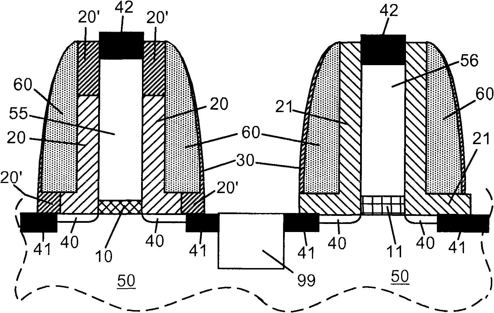
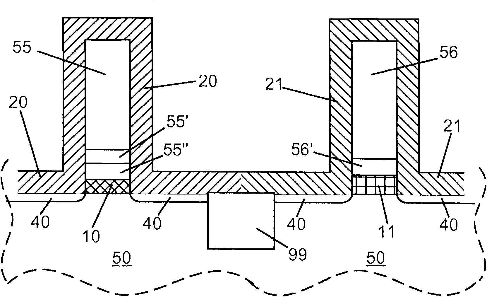
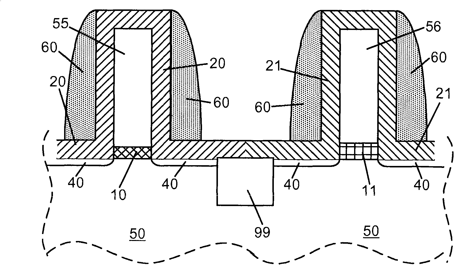
[0016] Field Effect Transistors (FETs) are considered well known in the field of electronics. The standard components of a FET are a source, a drain, a body between the source and drain, and a gate. The body is usually part of a substrate and is often referred to as the substrate. A gate covers the body and is capable of inducing a conduction channel in the body between the source and drain. In general nomenclature, channels are provided in the body. The gate is isolated from the body by a gate insulator. There are two types of FET devices: the hole-conducting type, known as a PFET; and the electron-conducting type, known as an NFET. Typically and exclusively, PFET and NFET devices on the same chip are wired as CMOS circuits. The CMOS circuit includes at least one PFET and at least one NFET device. When manufacturing or processing, when PFET and NFET devices are fabricated together on the same chip, you are actually dealing with CMOS processing and fabricating CMOS struct...


PUM


Abstract

A CMOS structure is disclosed in which a first type FET contains a liner, which liner has oxide (20) and nitride (20') portions. The nitride portions are forming the edge segments of the liner. Thesenitride portions are capable of preventing oxygen from reaching the high-k dielectric gate insulator (10) of the first type FET. A second type FET device of the CMOS structure has a liner without nitride portions (21). As a result, an oxygen exposure is capable to shift the threshold voltage of the second type of FET, without affecting the threshold value of the first type FET. The disclosure alsoteaches methods for producing the CMOS structure in which differing type of FET devices have their threshold values set independently from one another.

Description

technical field [0001] The present invention relates to electronic devices. More specifically, the present invention relates to CMOS structures having high-k gate dielectrics and methods of adjusting threshold voltage by exposing the gate dielectric to oxygen. Background technique [0002] Today's integrated circuits include an enormous number of devices. The two principles of smaller devices and reduced area are the keys to improving device performance and reducing cost. As FET (Field Effect Transistor) device dimensions scale down, the technology becomes more complex, requiring changes in device structure as well as new fabrication methods to maintain the expected performance increase from one device generation to the next. The primary material in microelectronics is silicon (Si), or more broadly, silicon-based materials. One such silicon-based material of considerable importance to microelectronics is the silicon-germanium (SiGe) alloy. The devices in the embodiments ...

Claims


Application Information

Patent Timeline
Patent Type & Authority Applications(China)
IPC IPC(8): H01L27/092H01L21/8238
CPCH01L27/092H01L21/28176H01L21/823857H01L29/4983H01L29/6653H01L21/823864H01L29/517H01L29/6656H01L21/18H01L21/8238
Inventor C·D·亚当斯E·A·卡蒂尔B·B·多里斯V·纳拉亚南
Owner IBM CORP
Why Eureka
Try Eureka