Window type semiconductor packaging structure capable of avoiding stripping in mold flow inlet

A technology of semiconductor and mold flow, which is applied in the direction of semiconductor devices, semiconductor/solid-state device components, electric solid-state devices, etc. It can solve problems such as stress deformation or peeling, affecting the reliability of finished products and manufacturing pass rate, and narrow mold flow entrance

Inactive Publication Date: 2010-03-17
POWERTECH TECHNOLOGY
View PDF0 Cites 4 Cited by
  • Summary
  • Abstract
  • Description
  • Claims
  • Application Information

AI Technical Summary

Problems solved by technology

[0004] In addition, China Taiwan Province Invention Patent Certificate No. I291751 proposes a packaging structure to prevent the die-bonding glue from contaminating the chip pads. A solder shield is formed on both sides of the line groove hole to prevent the die-bonding adhesive from contaminating the chip pad during die-bonding, but for the stress deformation or peeling of the die-bonding layer on both sides of the die-flow inlet caused by the impact of the mold flow The problem cannot be effectively solved
Furthermore, since the solder resist layer covers both ends of the slot hole (including the mold flow inlet), the mold flow inlet becomes narrower, and the adverse effect of the mold flow pressure impacting the die-bonding layer on both sides of the mold flow inlet is greater. Affected the reliability and manufacturing pass rate of finished products

Method used


Image

  • Window type semiconductor packaging structure capable of avoiding stripping in mold flow inlet
  • Window type semiconductor packaging structure capable of avoiding stripping in mold flow inlet
  • Window type semiconductor packaging structure capable of avoiding stripping in mold flow inlet

Examples


Embodiment Construction

[0050] Embodiments of the present invention will be described in detail below in conjunction with the accompanying drawings. However, it should be noted that these drawings are simplified schematic diagrams, and are only used to illustrate the basic structure or implementation method of the present invention, so only those related to the present invention are shown. The components shown are not drawn with the number, shape and size ratio of the actual implementation. Some size ratios and other related size ratios have been modified, enlarged or simplified to provide a clearer description. The number, shape and size of the actual implementation The size ratio is an optional design, and the detailed component layout may be more complicated.

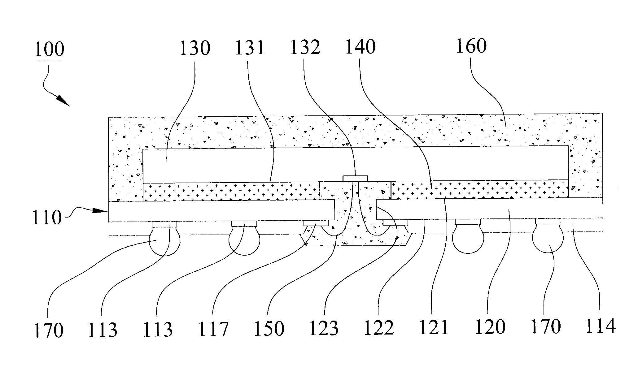
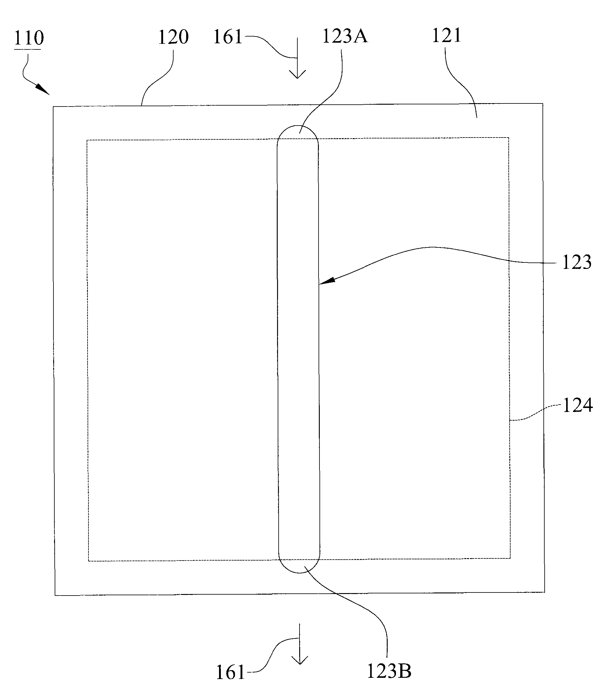
[0051] According to a specific embodiment of the present invention, a window-type semiconductor package structure that avoids mold flow inlet peeling is illustrated in image 3 Schematic cross-section of the die flow inlet cut along the sid...


PUM


Abstract

The invention discloses a window type semiconductor packaging structure capable of avoiding stripping in mold flow inlet, which mainly comprises a substrate, a chip of which the active surface is adhered onto the substrate, a chip adhering layer adhering the chip and the substrate core layer of the substrate, two or more weld lines and a mold sealing colloid. One end of a slotted hole of the substrate is formed into a mold flow beyond the chip; two or more mold flow restraining blocks are attached to the substrate core layer and positioned in places where the edge of a chip adhering zone meetsthe two sides of the slotted hole and slightly protrudes from the two sides of the mold flow inlet to restrain the impact of the mold flow on the mold sealing colloid from causing the stress of the chip adhering layer to avoid stripping in the mold flow inlet and maintain a chip adhesion clearance.

Description

technical field [0001] The present invention relates to a semiconductor device, in particular to a window-type semiconductor package structure that prevents mold flow inlets from being peeled off. Background technique [0002] In the existing semiconductor packaging structure, the chip is adhered on the substrate with a die-bonding layer, and the chip is sealed with a molding compound. When the substrate is provided with a window for internal electrical connection, the molding compound should be able to be formed on the substrate and in the window. There will be a narrow mold flow inlet between the upper surface of the substrate and the window, so the injection pressure when forming the molding compound will exert impact stress on the die-bonding layer on both sides of the mold-flow inlet, resulting in volume compression of the die-bonding layer Or deformation, or even intrusion into the bonding interface, affecting the packaging quality. [0003] see figure 1 As shown, a...

Claims


Application Information

Patent Timeline
Patent Type & Authority Applications(China)
IPC IPC(8): H01L23/488H01L23/498H01L23/13H01L23/31
CPCH01L2924/15311H01L2224/4824H01L2224/32225H01L2224/73215H01L2924/181
Inventor 李庄发吕肇祥邱政贤
Owner POWERTECH TECHNOLOGY
Why Eureka
Try Eureka