Encapsulating method and encapsulating module for LED chip

A technology of LED chip and packaging method, which is applied in the direction of electrical components, electric solid devices, circuits, etc., to achieve excellent heat dissipation characteristics, high optical characteristics, and reduce the effect of thermal interface

Inactive Publication Date: 2010-03-24
上海科学院 +1
View PDF0 Cites 15 Cited by
  • Summary
  • Abstract
  • Description
  • Claims
  • Application Information

AI Technical Summary

Problems solved by technology

This method reduces the thermal interface of the LED package and improves heat dissipation to a certain extent, but the solder wires are exposed on the substrate, and there are still certain problems in reliability.

Method used


Image

  • Encapsulating method and encapsulating module for LED chip
  • Encapsulating method and encapsulating module for LED chip
  • Encapsulating method and encapsulating module for LED chip

Examples


no. 1 example

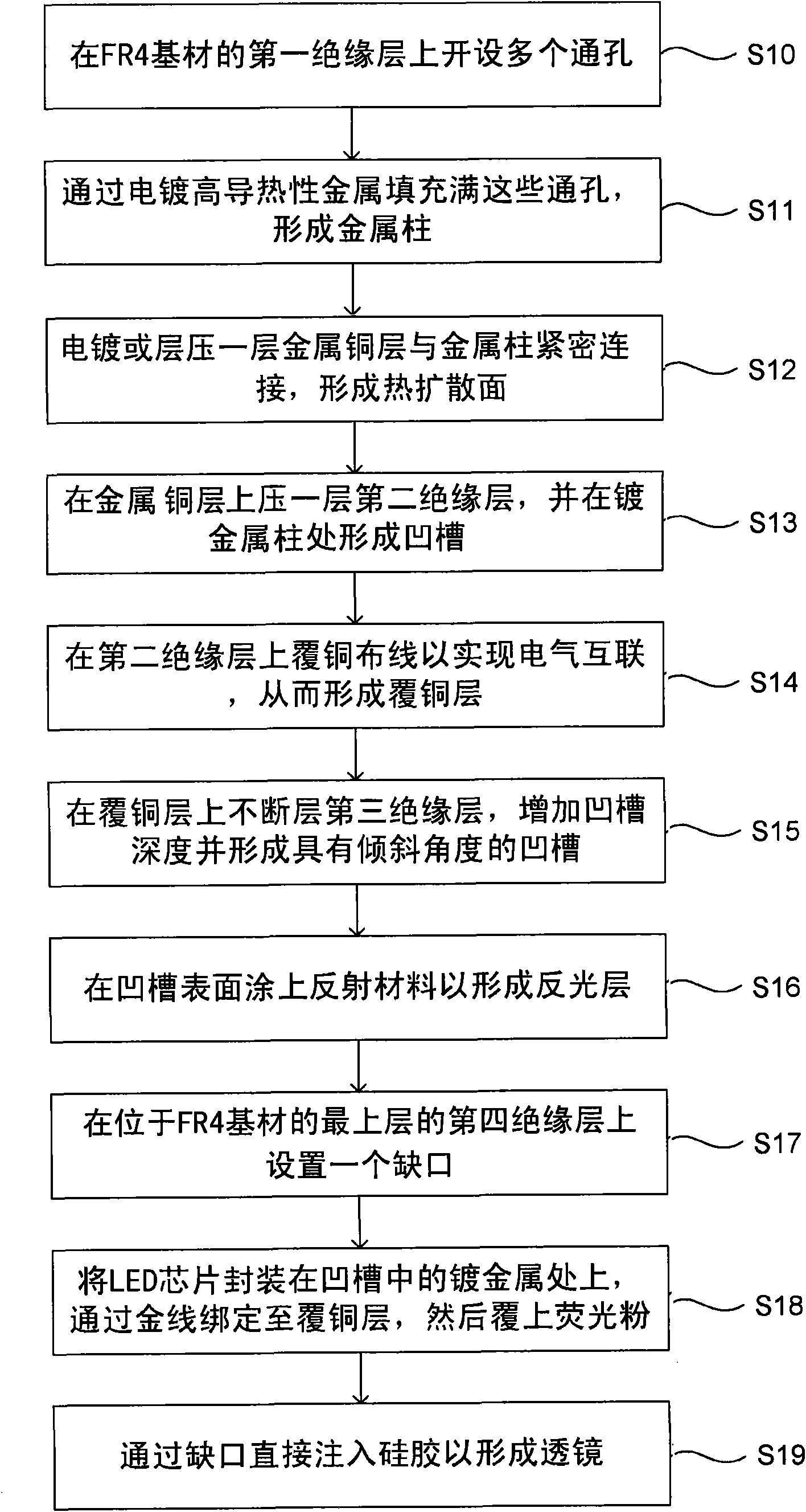
[0046] image 3 The flow of the first embodiment of the LED chip packaging method of the present invention is shown. See image 3 , the following is a detailed description of each step of the LED chip packaging method of this embodiment.

[0047] Step S10: opening a plurality of through holes on the first insulating layer of the FR4 substrate. The respective through holes may be spaced an equal distance apart.

[0048] Step S11 : filling these through holes with electroplating metal with high thermal conductivity to form metal pillars. Generally speaking, electroplated copper is used to fill these via holes to form copper pillars.

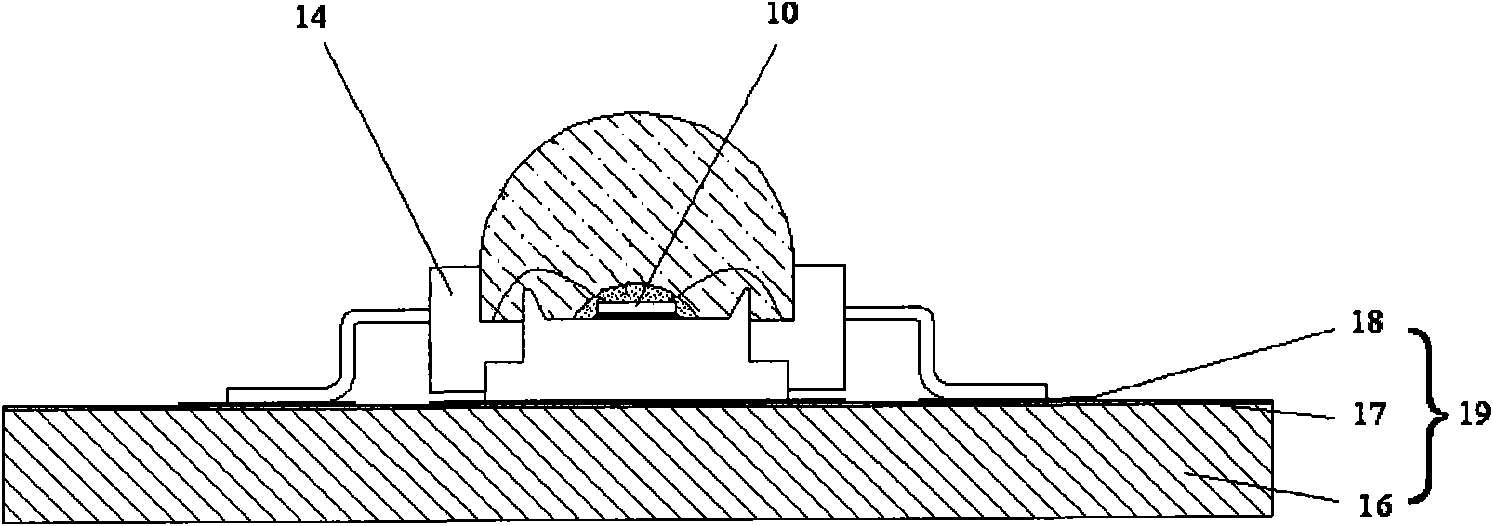
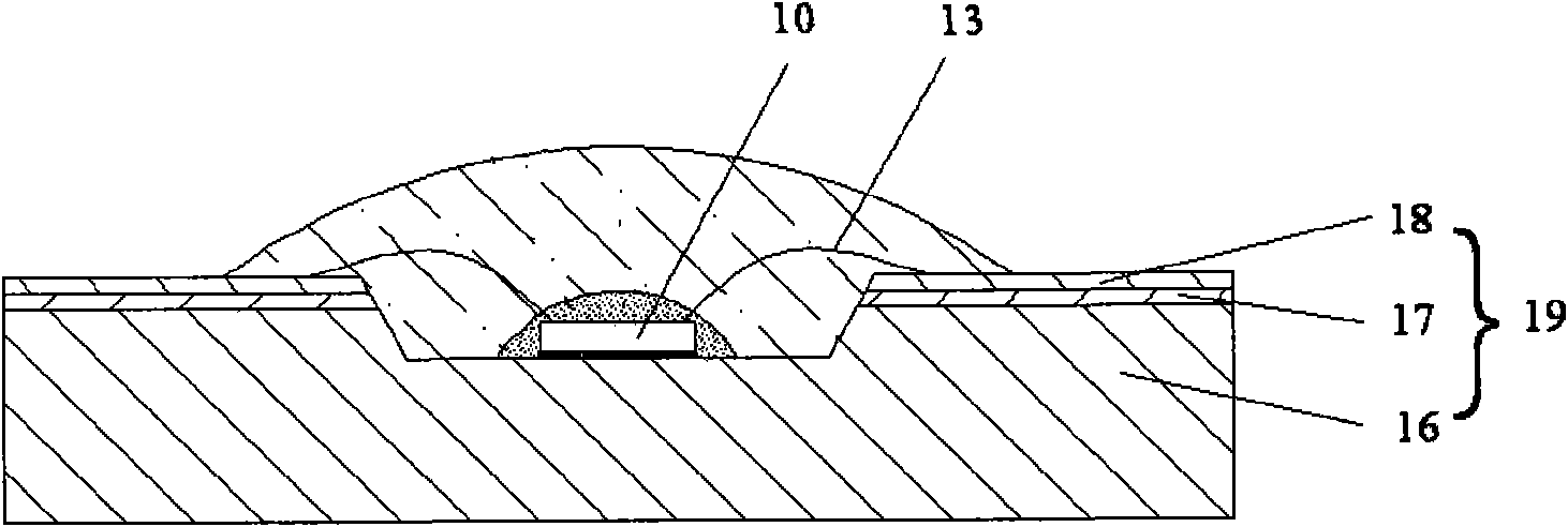
[0049] Step S12: electroplating or laminating a metal copper layer, and closely connecting with the metal pillars to form a heat diffusion surface.

[0050] Step S13: laminating a second insulating layer on the metal copper layer, and forming grooves at the metal-plated posts.

[0051] Step S14 : cladding copper wiring on the second insulatin...


PUM


Abstract

The invention discloses an encapsulating method and an encapsulating module for an LED chip, solving the problems of heat dissipation and cost of LED encapsulation application. The technical scheme ofthe invention is that the method comprises the following steps: opening at least one through hole on a first insulating layer of a FR4 base material; filling the through hole through electroplating high-thermal conductive metal to form a metal column; electroplating or laminating a metal copper layer to be closely connected with the metal column to form a heat diffusing surface; pressing a secondinsulating layer on the metal copper layer, and forming a groove at the part of plating the metal column; coating copper cabling on the second insulating layer by electrical interconnection to form acopper coating layer; constantly laminating a third insulating layer on the copper coating layer, and increasing depth of the groove, and forming a groove with an inclined angle; coating a reflectionlayer on the surface of the groove; arranging a gap on a fourth insulating layer on the uppermost layer of the FR4 base material; encapsulating the LED chip on the metal plated position in the groove, binding the LED chip to the copper coating layer through gold threads, and coating phosphor powder on the LED chip; and injecting silica gel on the LED chip to form a lens. The method is applicablein the filed of LED chip encapsulation.

Description

technical field [0001] The invention relates to a packaging method and a packaging structure of an LED chip, in particular to a COB (Chip On Board) packaging method and a packaging module of a high-power white LED chip. Background technique [0002] The packaging structure of existing high-power LED chips is as follows: figure 1 As shown, the high-power LED chip 10 is packaged on a copper-based support 14 to form a single light-emitting device. In application, the LED chip 10 is soldered to the substrate 19 . The surface of the metal substrate 16 is covered with an insulating layer 17 and a copper clad layer (also referred to as a wiring layer) 18 made of copper foil. The LED chip 10 is electrically connected to the copper clad layer 18 through solder. The metal substrate 16 is generally made of high thermal conductivity metals such as aluminum and copper, and the insulating layer 17 is generally made of polymer materials. Due to the presence of multiple thermal interfac...

Claims


Application Information

Patent Timeline
Patent Type & Authority Applications(China)
IPC IPC(8): H01L33/00H01L21/48H01L21/50H01L23/367H01L23/498
CPCH01L2924/0002H01L2224/8592H01L2224/48091H01L2224/48247H01L2924/181H01L2924/00014H01L2924/00012
Inventor 袁柳林
Owner 上海科学院
Why Eureka
Try Eureka