
Method for designing micro/nano-scale nonstandard product structure

A technology of product structure and micro-nano scale, applied in the direction of micro-structure technology, micro-structure devices, computing, etc., can solve the problem of the scale and complexity of micro-nano-scale product design, and the difficulty of macro-scale design methods to adapt to micro-nano scale and limitations. Issues such as product independence and innovation, to achieve the effect of improving design efficiency, enhancing openness, and meeting simulation needs

Inactive Publication Date: 2010-05-12
ZHEJIANG UNIV
View PDF0 Cites 5 Cited by
  • Summary
  • Abstract
  • Description
  • Claims
  • Application Information

AI Technical Summary

Problems solved by technology

[0004] It can be seen that the design scale and design complexity of micro-nano scale products are getting higher and higher, and the time-consuming simulation and analysis has become a bottleneck restricting innovative design.
On the other hand, most of the existing micro-nano-scale product designs are based on parametric cell libraries, and it is difficult to realize direct system-level design of non-standard and non-library complex devices, which greatly limits the autonomy and innovation of products
The macro-scale design method is difficult to adapt to the micro-nano scale, especially the design of non-standard structures. To solve this problem, a micro-nano scale non-standard product structure method is proposed

Method used


Image

  • Method for designing micro/nano-scale nonstandard product structure
  • Method for designing micro/nano-scale nonstandard product structure
  • Method for designing micro/nano-scale nonstandard product structure

Examples


Embodiment Construction

[0031] The present invention will be further described below in conjunction with the accompanying drawings and embodiments.

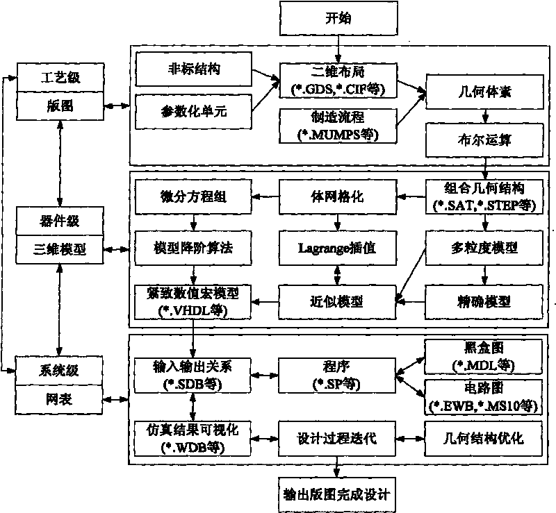
[0032] Such as figure 1 Shown is the main design process of the method proposed by the present invention. The interface from device level to system level is called macro modeling. The macromodel connects the device-level model and the system-level model. The modeling level of micro-nano structure can be divided into system level, device level and process level design.

[0033] (1) System-level design: Facing user requirements, focusing on the overall behavioral characteristics and performance of the system, including product concept design, formulation of design schemes, providing basis for device-level design, and integrating the macro-model obtained at the device layer into the system model Carry out simulation and optimize the system according to the simulation results.

[0034] (2) Device-level design: including device modeling, process simulati...


PUM


Abstract

The invention discloses a method for designing a micro / nano-scale nonstandard product structure. The method comprises the following steps: acquiring a device-level nonstandard three-dimensional structure through a two-dimensional layout of the nonstandard structure and a definition file of a manufacturing flow; establishing a complete finite element model, and mapping, extracting and describing the integral quality, rigidity and damping matrix of a system to acquire a system-level model; selecting a mode as an analysis object, and using an initial position or a test load as an input vector so as to acquire an output vector; based on the input / output vector, acquiring a system-level coarse-grained model through Lagrange interpolation; adjusting the granularity of the model, and mapping the matrix to low-dimensional space till the residual error meets the precision requirement so as to acquire a compact numerical value macro model; and after the design object meets the requirement, exporting layout information, and finishing the nonstandard product design. The method expands the design of simple devices limited in cell libraries to independent design supporting complex fantastic nonstandard products, and is favorable for improving the design quality and efficiency of the micro / nano-scale independent products.

Description

technical field [0001] The invention relates to a product digital design method, in particular to a micro-nano-scale non-standard product structure design method. Background technique [0002] With the development of micro-electro-mechanical system technology, in the fields of information communication, medical biology, automobile and other fields, the demand for the design of micro-nano scale product structure is increasing day by day. Research on the integration and compound design and manufacturing technology of micro-nano structure is of great significance to improve the competitiveness in the production field. [0003] Micro-nano-scale product structure design is different from macro-scale product structure design. The difference is that the former generally involves scale effects and multi-field coupling issues. Generally, the scale larger than 1 mm is called the macro scale, the scale of 1 μm-1 mm is called the micro scale, and the scale of 0.1 nm-100 nm is called th...

Claims


Application Information

Patent Timeline
Patent Type & Authority Applications(China)
IPC IPC(8): G06F17/50B81C99/00
Inventor 张树有谭建荣
Owner ZHEJIANG UNIV
Learn More