Eliminator for parasitic inductance of smoothing capacitor

A technology of filtering capacitors and parasitic inductance, which is applied in the field of elimination devices for parasitic parameters of components, can solve problems such as affecting the elimination effect and secondary parasitic effects, achieves convenient control, reduces the influence of high-frequency characteristic improvement, and reduces the positive area small effect

Inactive Publication Date: 2010-05-12
NANJING UNIV OF AERONAUTICS & ASTRONAUTICS
View PDF1 Cites 5 Cited by
  • Summary
  • Abstract
  • Description
  • Claims
  • Application Information

AI Technical Summary

Problems solved by technology

Figure 3B It is a cross-sectional view along the M-N line, the upper and lower coils 301 and 302 are distributed oppositely, and the distributed capacitance C between them is 31 Larger, so it will bring about secondary parasitic effects and affect the elimination effect

Method used


Image

  • Eliminator for parasitic inductance of smoothing capacitor
  • Eliminator for parasitic inductance of smoothing capacitor
  • Eliminator for parasitic inductance of smoothing capacitor

Examples


Embodiment Construction

[0027] The technical solution of the present invention will be described in detail below in conjunction with the drawings:

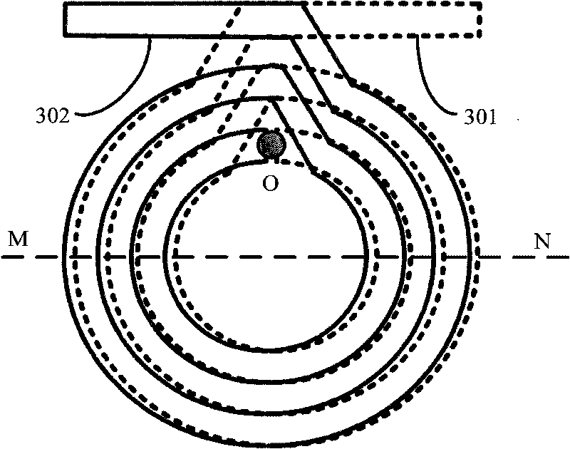
[0028] Such as Figure 4A In the example shown, the device for eliminating parasitic inductance of a capacitor provided by the present invention includes a PCB board 401 on which a capacitor 404 is mounted, two PCB winding coils 402 and 403, the coils are respectively on the upper and lower layers of the PCB, and It is forward coupling, that is, the end A of the upper coil 402 and the end C of the lower coil 403 are the same-named ends, and the B and C ends are connected by the via E. The pins G and H of the capacitor 404 are respectively mounted on the via holes E and F. According to the above connection, the parasitic inductance of the capacitor can be eliminated.

[0029] Figure 4B for Figure 4A The equivalent circuit diagram, the inductance values ​​of the upper and lower PCB coils 402 and 403 are respectively L 41 And L 42 , M 41 Is mutual inductance, ...


PUM


Abstract

The invention provides an eliminator for parasitic inductance of a smoothing capacitor, which comprises a printed circuit board (401), and an upper layer plane helical coil (402) and a lower layer plane helical coil (403) which are arranged on the printed circuit board (401). The upper layer plane helical coil and the lower layer plane helical coil are formed by connecting im semi-circular PCB windings end to end of which semi-diameters are increased successively; the semi-circular PCB windings with the same semi-diameter are symmetrical about mirror image, so that the upper layer plane helical coil and the lower layer plane helical coil are in staggered arrangement; the upper layer plane helical coil is connected in series with the lower layer plane helical coil through a through hole E which is formed on the printed circuit board (401) to form an orthodromic coupled structure, namely, the directions of currents in the upper layer plane helical coil and the lower layer plane helical coil are the same. The through hole E is also used for accommodating a pin of the capacitor; the values of mutual inductance and the parasitic inductance are the same by controlling the number of the semi-circular PCB windings in the upper layer plane helical coil and the lower layer plane helical coil according to the parasitic inductance value of the capacitor.

Description

Technical field [0001] The invention relates to a device for eliminating parasitic parameters of components, in particular to a device for eliminating parasitic inductance of a filter capacitor. Background technique [0002] The capacitor works under high frequency conditions, and its equivalent model is determined by its own capacitance C 11 , Equivalent inductance L 11 And equivalent resistance R 11 Series composition, such as figure 1 Shown. Due to the presence of parasitic inductance, resonance occurs on the capacitor branch, and the impedance characteristic above the resonance frequency is inductive, which makes the bypass effect of the capacitor on high-frequency noise abruptly reduced, thereby reducing the high-frequency performance of the capacitor. [0003] In order to improve the high frequency characteristics of capacitors, scholars at home and abroad have done a lot of research on the elimination of capacitor parasitic inductance, especially the elimination of capacitor...

Claims


Application Information

Patent Timeline
Patent Type & Authority Applications(China)
IPC IPC(8): H03H1/00
Inventor 崔永生王世山周小林武丽芳
Owner NANJING UNIV OF AERONAUTICS & ASTRONAUTICS
Why Eureka
Try Eureka