Method for manufacturing double-sided hollow flexible circuit board

A technology of flexible circuit boards and manufacturing methods, which is applied in the fields of printed circuit manufacturing, printed circuits, electrical components, etc., and can solve the problem of poor coincidence of the upper and lower copper foils at the hollowed-out terminal parts, the thickness of the hollowed-out parts of the terminals cannot be made very thin, and the hollowed-out terminals Poor part accuracy and other problems, to achieve a high pass rate, suitable for mass production, and ensure the effect of firmness

Inactive Publication Date: 2010-05-19
昆山市线路板厂
View PDF0 Cites 7 Cited by
  • Summary
  • Abstract
  • Description
  • Claims
  • Application Information

AI Technical Summary

Problems solved by technology

The double-sided hollow flexible circuit board manufactured by the conventional double-sided flexible circuit board processing technology has poor coincidence of the upper and lower copper foils of the hollowed out terminal part, many burrs on the hollowed out edge, and poor accuracy of the hollowed out part of the terminal; due to the use of via holes To realize the conduction of the upper and lower copper foils of the hollowed out parts of the terminals, so the conductivity is poor, and because the double-sided substrate is used for processing, the thickness of the hollowed out parts of the terminals cannot be made very thin, usually controlled above 60 microns
In addition, there is an insulating layer between the copper foil and the copper foil in the hollow part of the terminal. Due to the poor thermal conductivity of the insulating layer, it is easy to cause poor welding and falling off.

Method used


Image

  • Method for manufacturing double-sided hollow flexible circuit board

Examples


Embodiment Construction

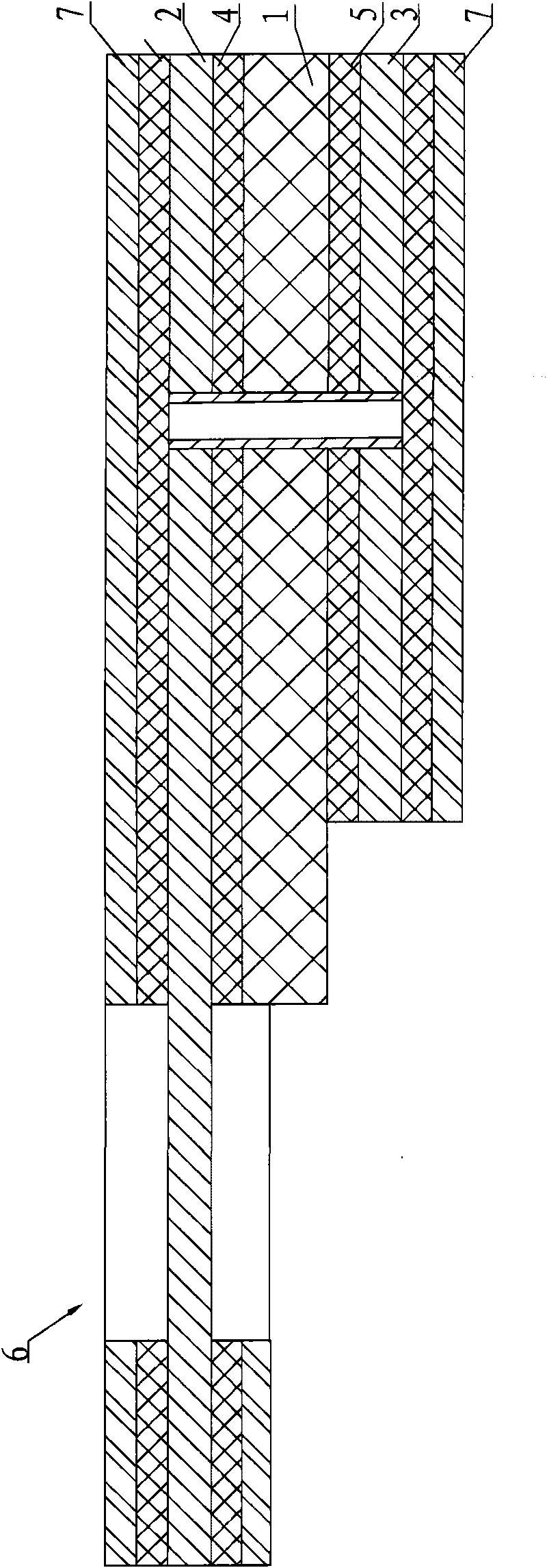
[0022] According to the manufacturing method of the double-sided hollow flexible circuit board of this embodiment, the following steps are sequentially included:

[0023] (1), take the first copper foil (18 microns thick), the first bonding board (semi-cured epoxy resin material, model MS13A, Shenzhen Shengming Electronic Materials Co., Ltd.), insulating material board (polyimide substrate ), the second bonding board, and the second copper foil (18 microns thick), the predetermined areas of the first bonding board, insulating material board and the second bonding board are punched out with a punching die to form the opening of the hollowed out part;

[0024] (2) Align the first copper foil, the first bonding board, the insulating material board, the second bonding board, and the second copper foil with the positioning holes one by one for fixing, and then place them in a vacuum laminator at a temperature of 100°C 1. The pressure is 10 kg / cm2 and the holding time is 30 minutes ...


PUM


Abstract

The invention relates to a method for manufacturing a double-sided hollow flexible circuit board. The method adopts manufacturing technology of laminating materials, and comprises the following steps: firstly, performing die cutting by a punching mould to remove an insulation layer which is not needed by a hollow part; then, performing lamination and pressing on needed copper foil, bonding material and insulation material by a vacuum laminator; and finally, adopting a routine flexible double-sided plate manufacturing process to realize conduction and form a pattern. The double-sided hollow flexible circuit board manufactured by the method has the advantages of reliable connection of the hollow part, low defective index, high production efficiency, stable welding performance, reliable work and the like, overcomes poor phenomena that a traditional production process has poor consistency of products, high defective index, low machining speed, fussy machining process, poor welding and easy falling off of the hollow connecting part and the like, really ensures the quality of the products and truly achieves ultimate effects of persistent high efficiency and stability.

Description

technical field [0001] The invention relates to a method for manufacturing a circuit board, especially a double-sided hollow flexible circuit board. Background technique [0002] In the prior art, when the double-sided hollowed out flexible circuit board is processed, the processing technology of the conventional double-sided flexible circuit board is still adopted, that is, the copper foil of the hollowed-out terminal part is etched with the base material of the double-sided board through an etching process. Graphic etching molding, because this etching technology can only etch copper, but cannot etch away the insulating layer between copper and copper. Therefore, the hollow part of the final hollow terminal part needs to be hollowed out with a punching tool Part of the punching is removed, and in order to make the upper and lower copper foils of the hollow terminal part conductive, it is necessary to drill a hole between the upper and lower copper foils of the hollow termi...

Claims


Application Information

Patent Timeline
Patent Type & Authority Applications(China)
IPC IPC(8): H05K3/00
Inventor 张钧民严浩
Owner 昆山市线路板厂
Why Eureka
Try Eureka