Method for testing service life of NMOS hot carrier injection

A hot carrier and lifetime technology, applied in the direction of single semiconductor device testing, semiconductor/solid-state device testing/measurement, etc., can solve the problems of scrapped wafers and increased costs, and achieve cost saving, saving capacity and material loss, and saving The effect of test time

Active Publication Date: 2010-06-09
HEJIAN TECH SUZHOU
View PDF0 Cites 17 Cited by
  • Summary
  • Abstract
  • Description
  • Claims
  • Application Information

AI Technical Summary

Problems solved by technology

[0002] In the semiconductor manufacturing process, if there is an abnormality in the device on the production line, and the reliability of hot carrier injection (HCI) needs to be tested, it is usually obtained through package level testing. The lif

Method used


Image

  • Method for testing service life of NMOS hot carrier injection
  • Method for testing service life of NMOS hot carrier injection
  • Method for testing service life of NMOS hot carrier injection

Examples


Example Embodiment

[0017] The specific embodiments of the present invention will be described in more detail below in conjunction with the accompanying drawings.

[0018] A method for testing the hot carrier injection lifetime of an NMOS device includes the following steps:

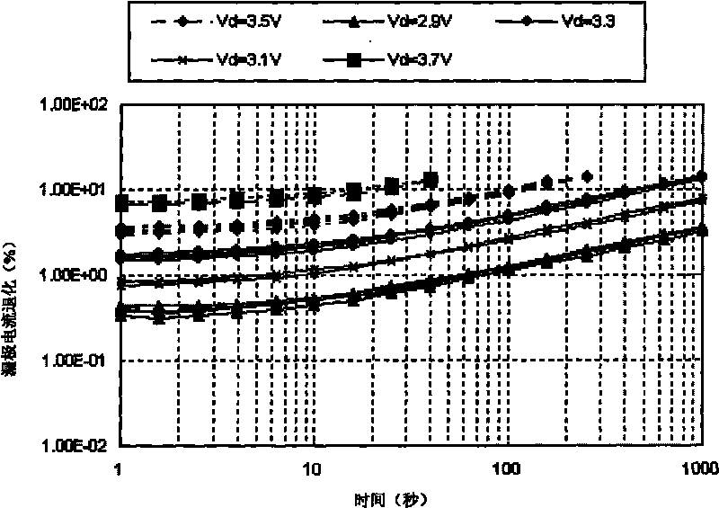
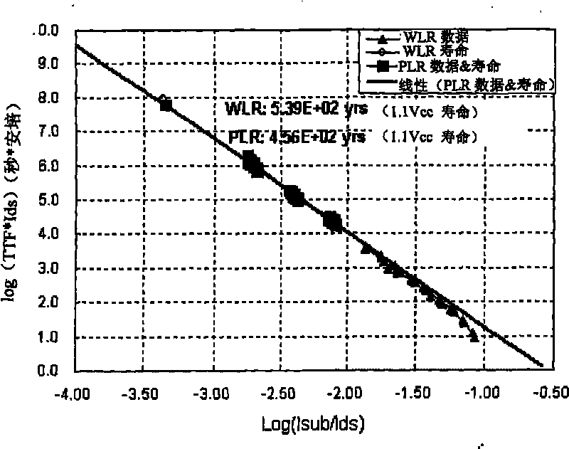
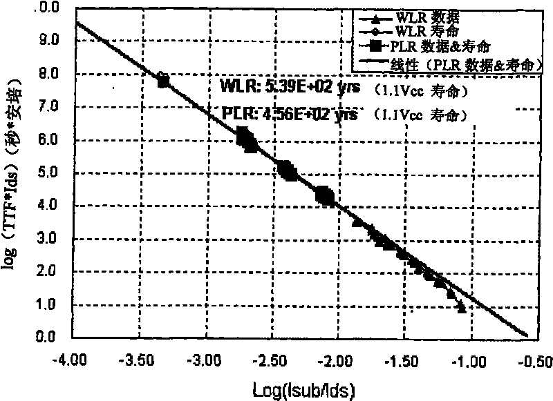
[0019] Step 1. The test system applies test voltage stress to the drain of the device under test, and the value of the test voltage is between 60% and 70% of the punch-through voltage. The test system can be determined as required. In this embodiment, the Agilent 4070 test system is used in the RMB (Agilent assembly language Rocky Mountain Basic, applied to the Agilent test system) environment; the stress voltage applied to the drain is the most important One of the parameters.

[0020] Step 2. The test system uses the maximum substrate current method to perform the test. The gate voltage corresponding to the maximum substrate current when the voltage stress is applied to the drain is the gate voltage stress, and the gate voltage...


PUM


Abstract

The invention relates to a method for testing the service life of NMOS hot carrier injection, which comprises the following steps that: 1, a test system applies a test voltage stress to a drain electrode of a tested apparatus, wherein the value of the test voltage accounts for 60 and 70 percent of value of a punch through voltage; 2, a grid voltage corresponding to a maximum substrate current when the voltage stress is applied to the drain electrode is a grid voltage stress, and the grid voltage stress is accessed to obtain a degradation picture of a drain electrode current of the tested apparatus; and 3, the test system fits data obtained by the step 2 to obtain a failure time of the tested apparatus, and when the apparatus is degraded to over 5 percent, the failure time of the apparatus is obtained through heterodyne calculation and then the service life of hot carrier injection is calculated by using a formula, namely TTF*Ids=C*(Isub/Ids)m. Through the technical scheme of the invention, the service life of the NMOS hot carrier injection can be quickly obtained so as to greatly shorten the test time and save the cost without packaging a chip.

Description

technical field [0001] The invention relates to semiconductor manufacturing technology, in particular to a method for testing NMOS hot carrier injection lifetime. Background technique [0002] In the semiconductor manufacturing process, if there is an abnormality in the device on the production line, and the reliability of hot carrier injection (HCI) needs to be tested, it is usually obtained through package level testing. The life of hot carrier injection, this test method not only needs to scrap the wafer, increase the cost, but also needs extra time to package the device, resulting in a test time of more than half a month to clarify the performance of hot carrier injection. Contents of the invention [0003] In view of the defects of the prior art, the purpose of the present invention is to propose a method for testing the life of NMOS hot carrier injection, which can quickly obtain the life of NMOS hot carrier injection, greatly shorten the test time, and does not need...

Claims


Application Information

Patent Timeline
IPC IPC(8): G01R31/26H01L21/66
Inventor 彭钦宏彭昶
Owner HEJIAN TECH SUZHOU
Why Eureka
Try Eureka