Eureka AIR delivers breakthrough ideas for toughest innovation challenges, trusted by R&D personnel around the world.

Bridgeless power factor correction converter with single inductance and three levels

A power factor correction and three-level technology, which is applied in the direction of converting AC power input to DC power output, high-efficiency power electronic conversion, and output power conversion devices, can solve the problem of increasing circuit complexity and cost, low device utilization, and Bulk and other problems, to achieve the effect of high device utilization, low conduction loss, and high conversion efficiency

Inactive Publication Date: 2010-06-09
ZHEJIANG UNIV
View PDF7 Cites 26 Cited by
  • Summary
  • Abstract
  • Description
  • Claims
  • Application Information

AI Technical Summary

Problems solved by technology

However, these bridgeless converters require two sets of Boost circuits to work in the positive and negative half cycles of the AC input voltage respectively, and only have one DC bus output, so the device utilization rate is low, the volume is large, and the cost is high; moreover, these bridgeless converters Or the common mode interference is large or cannot work in the current continuous mode (CCM), and additional power devices such as power diodes and inductors are required to improve performance, which increases the complexity and cost of the circuit

Method used


Image

  • Bridgeless power factor correction converter with single inductance and three levels
  • Bridgeless power factor correction converter with single inductance and three levels
  • Bridgeless power factor correction converter with single inductance and three levels

Examples


Embodiment Construction

[0018] The embodiment of technical scheme is described in detail with reference to accompanying drawing:

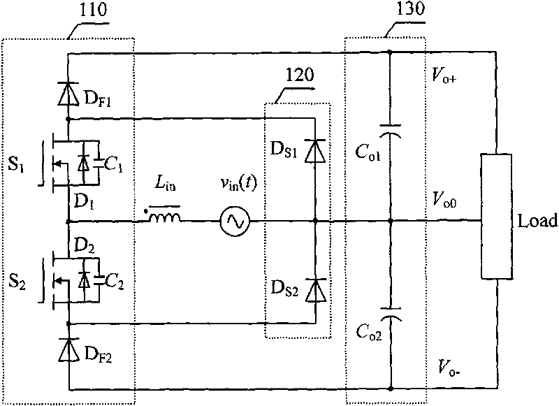
[0019] figure 1 Shown is a specific circuit diagram of the single-inductance three-level bridgeless power factor correction converter of the present invention. The converter includes an input inductor L in , Boost arm circuit 110, clamping circuit 120 and output voltage dividing capacitor 130.

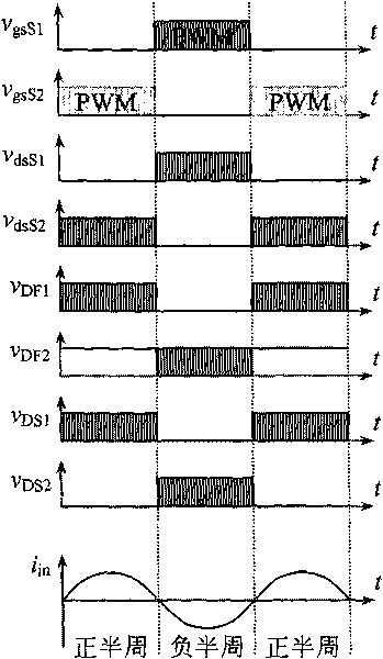
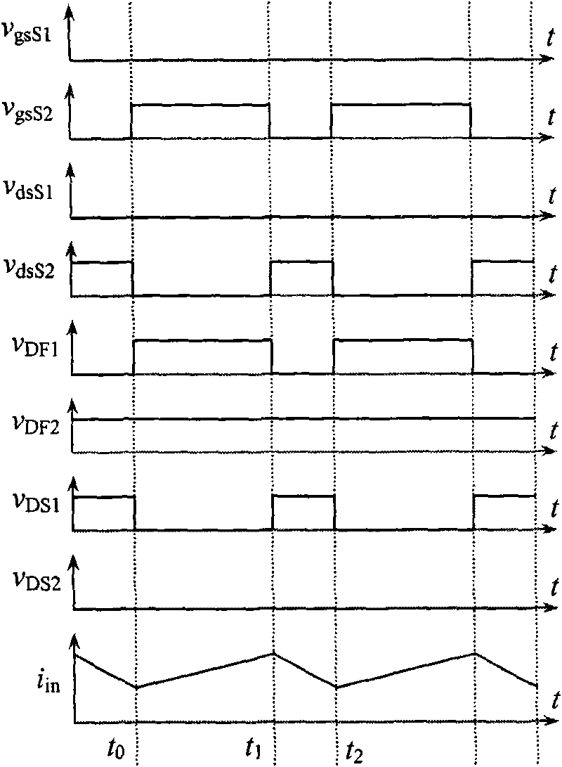
[0020] As shown in the figure, the Boost arm circuit 110 consists of two switch tubes S 1 , S 2 and two diodes D F1 、D F2 It is formed in series, with two diodes on the outside and two switches on the inside. where diode D F1 The anode of the switch tube S is connected to 1 The drain of the switch tube S 1 The source is connected to the switch S 2 The drain of the switch tube S 2 The source is connected to the diode D F2 of the cathode. Switch tube S in Boost arm circuit 110 1 , S 2 The switching operation is achieved on the inductance L in charging and discharging...


PUM


Abstract

The invention relates to a bridgeless AC / DC power factor converter with low on-state loss and aims to provide a bridgeless power factor correction converter with single inductance and three levels. The converter comprises an input inductance, a Boost arm circuit, a clamping circuit and an output voltage-dividing capacitor, wherein the Boost arm circuit is formed by connecting two switch tubes and two diodes in series. The two diodes are arranged at the outside of the Boost arm circuit, and the two switch tubes are arranged at the inside. An anode of the diode DF1 is connected with a drain electrode of a switch S1, a source electrode of the switch S1 is connected with a drain electrode of a switch S2, and a source electrode of the switch S2 is connected with a cathode of the diode DF2. The switch tubes of the Boost arm circuit are opened and closed, and then the charging and discharging on the inductance and the power factor correction of the input end are realized. The invention only needs one input inductance to obtain two negative and positive DC buses, and has the advantages of low stress and high utilization rate of the device, low on-state loss, low common-mode interference and high conversion efficiency.

Description

technical field [0001] The invention relates to a bridgeless AC / DC power factor converter with low on-state loss, in particular to a single inductance three-level bridgeless power factor correction converter. Background technique [0002] The current single-phase power factor correction technology generally adopts the traditional Boost power factor correction converter. This converter consists of two parts: rectifier bridge and Boost converter. The rectifier bridge rectifies the AC mains into a unidirectional voltage source; the Boost converter realizes power factor correction through a certain control method. This single-phase power factor correction converter is applied to the global universal power input (90VAC-264VAC), and can achieve power factor correction relatively well, but when it works in applications with low input voltage, the loss of this converter will increase. The large increase is mainly due to the rapid increase of on-state losses at low input voltages. ...

Claims


Application Information

Patent Timeline
IPC IPC(8): H02M7/217H02M1/42H02M1/44
CPCY02B70/126H02M1/4233H02M7/487Y02B70/10Y02P80/10H02M1/0085
Inventor 张军明苏斌吕征宇
Owner ZHEJIANG UNIV
Why Eureka
Eureka Blog
Learn More